Paolo Alagna, Gregory Rechtsteiner, Ivan Lalovic and Theodore Cacouris, Cymer LLC
Process- and technology-specific correlations can be established for better process control, and to prevent excursions.
As Moore’s law marches on, semiconductor manufacturers rely on advances in photolithography – the use of 193-nm ArF excimer lasers, for example, coupled with optical and process techniques to improve resolution and reduce patterning variations. Recent examples of such technologies include advanced reticle designs that correct for optical proximity effects, use of double- or multiple-patterning exposure methods, computational techniques that achieve source-mask optimization (SMO) and free-form scanner illumination technologies.1,2
These techniques all require increasing stability and control of the excimer laser performance.3,4 Experiments have shown that laser variations in energy, wavelength and bandwidth are well correlated to on-wafer results,2,5,6 and as the industry transitions to even smaller geometries, the stability of optical beam parameters such as divergence, pointing and polarization are also expected to impact process yields. It is important to accurately monitor critical performance indicators in real time to avoid misprocessing a larger number of semiconductor wafers. Until recently, light-source-performance monitoring has been limited primarily to a small set of parameters (energy, bandwidth and wavelength). In addition, real-time measurements of critical illumination parameters such as divergence, pointing and polarization have not been possible.
The SmartPulse light-source data collection and analysis tool from Cymer includes new real-time metrology. This capability significantly expands the existing metrology on excimer laser sources for semiconductor lithography, providing real-time beam parameter measurements during wafer exposures including far-field (pointing and divergence), near-field (energy density) and polarization components.7,8
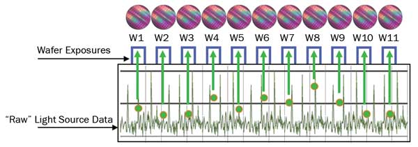
The tool enables chip makers to monitor and correlate laser performance with each wafer exposed and therefore identify potential sources of lithography patterning variability and prevent excursions. This is a significant enhancement over previous time-based data-sampling approaches, since it filters nonwafer exposure operation of the light source (e.g., calibrations and scanner prechecks), enabling improved correlation between light-source performance and wafer patterning (Figure 1). It makes this information available in real time and can be used to develop process- and technology-specific correlations to improve process control and prevent excursions, especially for divergence, pointing and polarization – parameters that have not been previously studied in this way.

Figure 1. SmartPulse: Laser metrology data is associated with each wafer, allowing chip makers to monitor and correlate laser performance with individual wafers, and to identify patterning variability and prevent excursions.
To quantify the impact that beam variations could have on the lithography process, Cymer, in collaboration with IMEC (the Interuniversity Microelectronics Center) in Louvain, Belgium, performed experiments on an XLR 560i excimer laser, operating as part of the ASML XT:1900i lithography cluster. Controlled changes in light-source beam divergence, pointing and polarization were introduced and measured, and various test wafers were exposed and measured. Three scenarios were created by varying the beam alignment conditions:
• Condition 1: Small divergence and pointing change.
• Condition 2: Large divergence and pointing change.
• Condition 3: Polarization variation.
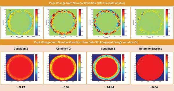
The resulting changes in laser beam parameter performance (Figure 2) are quantified in terms of differences from the nominal (or baseline) performance.

Figure 2. Controlled experiments quantified beam variations’ impact on lithography. Three different scenarios demonstrated varying beam alignment conditions: Condition 1 used small divergence and pointing change; Condition 2 used large divergence and pointing change; and Condition 3 used polarization variation. The resulting changes in laser beam parameter performance are quantified in terms of differences from the nominal (or baseline) performance.
The impact of wafer exposure on scanner illumination was tested for several off-axis and free-form illumination conditions at NA 1.35, targeting 41- to 45-nm nominal critical dimension (CD) for line-space and contact-hole patterns of 70 nm at different pitches.
The wafer-plane intensity for each experiment condition was measured, and changes in pointing, divergence and polarization changes significantly impacted the measured loss, with the largest reduction seen in the case of Condition 3. Illumination pupil measurements obtained by the scanner have been used to calculate the induced changes by comparing differences from each experiment condition to the nominal or baseline value. This provided qualitative and measurable pupil and metrology response information for each condition.
IMEC’s analysis indicates interesting differences between the responses of the measured illumination conditions. Direct correlations between the reduction of the wafer-plane power and the annular integrated percent pupil-energy variation are shown in Figure 3.

Figure 3. Comparing conventional and raw-data pupil analysis shows a direct correlation between the reduction of the wafer-plane power and the annular integrated percent pupil-energy variation.
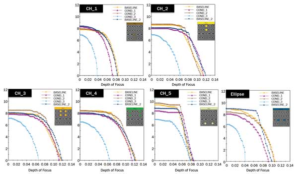
Analysis of the response of contact-hole patterning at the different beam conditions considered in this experiment was performed on a negative tone development process, the one optimized by IMEC for the experimental study of SMO for 22-nm design-rule SRAM cells.1 Six different contact-hole patterns in an SRAM layout were measured on wafers exposed across programmed variation in focus and dose. The nominal exposure dose was approximately 25 mJ/cm2.
Polarization and divergence variations (Condition 3) show the largest imaging impact. In this case, a CD change common for all six pattern targets, shown in Figure 4, was observed to be on the order of approximately +5 nm, with depth-of-focus reduction as large as 50 percent. This CD change can be translated to an effective focus and dose shift in this condition of approximately −20 nm in focus and −1 mJ/cm2 compared with the nominal (baseline) exposure condition.

Figure 4. Exposure latitude: response of diverse contact hole pitches to different light-source experiment conditions. A critical dimension (CD) change common for all six pattern targets was seen to be approximately +5 nm, with depth-of-focus reduction as large as 50 percent.
Line-space CD changes were also analyzed for each experimental condition. The results show a CD increase as a function of increasing pitch from dense (88-nm pitch) toward most contrast-sensitive semi-isolated patterns (400-nm pitch). Best focus at each condition was determined independently for the line-space measurements, but – unlike the contact process window measurements – no changes in best focus were observed in this case.
Figure 5 shows CD through-focus differences compared with the baseline of 0.25-0.5 nm for the 88-nm pitch; for contrast-sensitive semi-isolated patterns, it can reach up to 4 percent or 2 nm (45 nm of nominal CD at 200-nm pitch) over the c-quad and annular pupils tested.

Figure 5. Through-pitch CD change from nominal condition (measured at best focus); 88-nm pitch (left) and 200-nm pitch (right).
This analysis has been applied to all the pitches for two illumination sources, showing maximum impact on pitch 400 nm, where the maximum measured ?CD (through focus) is approximately 10 percent (~4 nm) from the nominal target at the baseline condition.
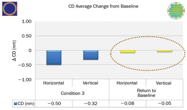
The CD uniformity across the wafer was also measured for the 400-nm pitch structure at best focus and nominal dose condition using annular illumination. The average across-wafer CD shows a difference between Condition 3 and baseline of approximately 0.5 nm (Figure 6), while the across-wafer CD uniformity increases by 0.7 nm in going from baseline to Condition 3 setting. Since other process factors (track, reticle and scanner/process fingerprint) are controlled between these wafer exposures, the most significant impact of the changes is related to the differences in light-source conditions.

Figure 6. The average across-wafer CD shows a difference between Condition 3 and baseline of approximately 0.5 nm.
Real-time monitoring can extend the understanding of how light-source parameters impact on-wafer patterning. With more complex SMO and free-form illumination schemes, it is clear that variation in divergence, pointing and polarization will have an impact on wafer-patterning quality, and that real-time monitoring can provide an advantage in process control and excursion prevention.
We have experimentally shown that divergence, pointing and polarization changes induced a significant impact on 22-nm design-rule SRAM contact holes using a negative tone development process, with a drift in CD as large as 5 nm across a range of device patterns. Effects were also measured on the patterning of line-space structures, where for contrast-sensitive patterns, a change in the 2- to 4-nm range (<10 percent) of nominal CD, with less than 1 percent dense line-space CD impact, was detected.
Meet the authors
Paolo Alagna is Europe application manager and Cymer’s assignee at IMEC; email: [email protected]. Gregory Rechtsteiner is director of data analytics at Cymer LLC; email: [email protected]. Ivan Lalovic is senior director of applications at Cymer; email: [email protected]. Theodore Cacouris is product marketing director at Cymer; email: [email protected].
Acknowledgments
The authors acknowledge the contributions of Koen D’havé, Lieve Van Look and Joost Bekaert from IMEC, as well as Omar Zurita and Joshua Thornes at Cymer, all of whom made this paper possible.
References
1. J. Bekaert et al (2010). Freeform illumination sources: an experimental study of source-mask optimization for 22-nm SRAM cells. Proc SPIE 7640, Optical Microlithography XXIII, 764008.
2. I. Lalovic et al (2007). Fast and accurate laser bandwidth modeling of optical proximity effects. Proc SPIE 6730, Photomask Technology 2007, 67301X.
3. R. Rokitski et al (2010). High reliability ArF light source for double patterning immersion lithography. Proc SPIE 7640, Optical Microlithography XXIII, 76401Q.
4. T. Cacouris et al (2012). Advanced light source technologies that enable high-volume manufacturing of DUV lithography extensions. Proc SPIE 8326, Optical Microlithography XXV, 83261G.
5. N. Seong et al (2008). Analysis of the effect of laser bandwidth on imaging of memory patterns. Proc SPIE 7140, Lithography Asia 2008, 714042.
6. U. Iessi et al (2010). Laser bandwidth effect on overlay budget and imaging for the 45nm and 32nm technology nodes with immersion lithography. Proc SPIE 7640, Optical Microlithography XXIII, 76402B.
7. P. Alagna et al (2013). Lithography imaging control by enhanced monitoring of light source performance. Proc SPIE 8683, Optical Microlithography XXVI, 8683OS.
8. J. Choi et al (2012). Enhancing lithography process control through advanced, on-board beam parameter metrology for wafer level monitoring of light source parameters. Proc SPIE 8326, Optical Microlithography XXV, 83262O.