Bertrand De Monte, e2v Technologies
Until recently, only photomultiplier tubes were suitable for low-light imaging. However, this technology and associated poor spatial resolution were not suited to scientific applications. Solid-state devices such as image intensifiers or electron-bombarded devices brought solutions to some key applications but have shown limitations such as poor modulation transfer function, low quantum efficiency or degradation at high light levels.
But now, electron-multiplying amplification can be used to enable enhanced imaging in minimal or high light. One system, the L3Vision CCD from e2v, enables improved performance with blue response and low cost.
The amplification process comes from excitation of electron-hole pairs by impact ionization. Tuning electron-multiplying input voltage tunes the amplification gain from 1x up to 1000x. As a result, a wide range of light levels can be covered, from daylight to the lowest photon flux.
The technology pushes light-level boundaries and can be employed in a wide range of markets, such as spectroscopic, scientific or lidar applications. A detector incorporating e2v’s L3Vision CCD technology recently was designed, manufactured and characterized for use in lidar applications.
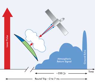
The L3Vision CCD was designed for possible use as the detector in a space-based lidar instrument with a 667-ns temporal sampling window to yield 100-m spatial resolution. A simplified overview of the instrument and its operation is shown in Figure 1. Use with a 355-nm laser required high quantum efficiency at ultraviolet wavelengths, necessitating a back-illuminated CCD structure.

Figure 1. Lidar system overview. Images courtesy of e2v technologies.
The detector’s architecture used high-speed charge binning to combine signals from each sampling window into a single charge packet. This was then passed through a multiplication register (electron-multiplying CCD) operating with a typical gain of 100x to a conventional charge detection circuit. The detector achieved a typical quantum efficiency of 80 percent and a total noise in darkness of <0.5 e— rms.
Electron-multiplication register
To achieve the required noise performance, it was predicted that multiplication gains in the range from 50 to 200 would be required. This range is readily achieved with a gain register similar to that used on previous e2v technologies designs, typically using 500 multiplication stages.
The stability of the multiplication gain was reviewed, as this depends on temperature and operating voltages, which are a very strong function of the amplitude of the high-voltage clock pulse (RØ2HV). Analysis of results from other devices suggested that a temperature stability of ±0.25 °C and a voltage stability of 4 mV would be necessary to achieve the required gain stability. Part of the characterization phase of the program was to demonstrate that these levels are achievable. Comparison with other devices suggested also that the required levels of linearity should be achievable with a standard register design for the system signal levels and the range of gains discussed above.
To allow calibration of the multiplication gain and measurement of linearity, an electrical input structure at the start of the gain register was proposed, based on similar structures that had been used on test devices produced by e2v. Electrical input was preferred rather than optical methods, as it allows better control and charge measurement for calibration.
It is known that, for a fixed high-voltage register clock amplitude, the on-chip multiplication gain drops as the device is run. This process is known as aging and depends on the total quantity of charge transferred through the multiplication register. To maximize the useful life of the sensor, it is important to ensure that only the wanted signals are passed through the register. The low duty cycle of the system, 400 signal samples in 10 ms, should ensure a tolerable level of aging over the mission lifetime.
Signal collection from 120-μm detector
Charge generated within the 120-µm-square detector area in a 667-ns interval must be combined into a single CCD element at the input of the gain register. This process must minimize the crosstalk between successive temporal samples. Charge transfer across a single pixel of this dimension would be extremely slow, particularly at the very low signal levels (~1 e— per sample) at which the sensor was required to operate.
To achieve the required performance, a number of architectures were considered, but it was concluded that the lowest risk was the use of conventional clocked binning of charge in an array of smaller pixels. This has the secondary advantage that the sensor area can be operated in a conventional imaging mode for alignment and other purposes.
The number and size of the pixels into which the detector is divided were determined by the trade-off between clock frequency and transfer efficiency. A larger number of smaller pixels requires a higher clock frequency to read out in the available time. A smaller number of larger pixels will have decreased transfer efficiency due to the slower charge transit time, which increases approximately as the cube of the pixel dimension.
A 6 x 6-pixel array of 20-µm-square pixels was calculated to be optimum. This pixel size allows clocking at 24 MHz with good transfer efficiency, which enables six image and two overscan pixels to be binned within a 667-ns sample period, with sufficient time remaining for the other required clocking.
For typical levels of charge transfer efficiency, the crosstalk between successive temporal samples of the optical signal is dominated by the “frame shift smear” in the image section. A model developed to calculate this for a range of optical spot sizes and positions confirmed that the specified value of 13 percent could be met.

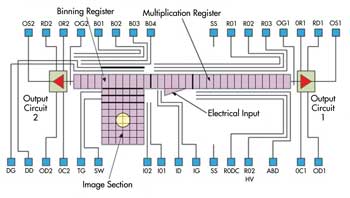
Figure 2. This schematic shows the architecture of L3Vision CCD technology.
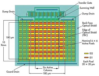
In Figure 2, the image section consists of a central 6 x 6-pixel array with additional rows and columns to minimize edge effects, as shown in Figure 3. Charge from the additional columns on each side is directly dumped to drains next to the binning register (not shown in the schematic). The image section has a total of 10 rows with the photosensitive region defined by a metal light shield, which is deposited directly on the CCD. Two-phase clock electrodes are used to simplify the high-speed clocking required to perform charge binning. Charge from the whole image section is binned into a summing well adjacent to the binning register but isolated from it by a separately clocked transfer gate.

Figure 3. This diagram demonstrates the architecture of the image section.
Lidar mode operating sequence
An overview of the lidar mode operation is shown in Figure 4. During the standby period, the image section is clocked with the dump gate held high to clear unwanted charge to the dump drain. In the acquisition period, photogenerated charge is integrated in the image section and rapidly binned vertically into the summing well. This integration and binning occur in a first 667-ns sample period.
During a second sample period, while the second sample signal is integrated, the first sample is transferred to the binning register. The first sample is binned horizontally into the gain register, while the second sample is binned into the summing well. During each following sample period, the first sample signal is advanced one stage along the gain register and multiplied.
 Figure 4. Lidar mode overview.
When the required set of 400 samples has been acquired into the multiplication register, the device is switched to readout mode. In this mode, the clocking of the multiplication register continues with the same timing, but the image and binning register clocks are stopped to avoid feedthrough into the output video waveform.
After readout is completed, the device returns to standby mode. The multiplication register is clocked continuously with a constant duty cycle throughout the entire sequence to facilitate maintaining a stable amplitude of, typically, 40 V, as required to yield a gain of 100x.
The electron-multiplying amplification process enables enhanced imaging in minimal light with systems such as the L3Vision CCD, overcoming the spatial resolution limitations of photomultiplier tubes as well as the modulation transfer function, quantum efficiency and degradation issues of solid-state devices such as electron-bombarded devices or image intensifiers. The electron-multiplying amplification process also enables a better blue response and lower cost.
Meet the author
Bertrand De Monte is marketing manager for e2v’s imaging division in Grenoble, France; e-mail: [email protected].