Rajesh S. Patel, Ashwini Tamhankar and Tim Edwards, Spectra-Physics, a Division of Newport Corp.
The green movement, energy conservation
efforts and global warming headlines have made the world aware of the need for more
energy-efficient lighting alternatives. The range of applications for high-brightness
LEDs continues to expand. Laser scribing of wafers used to make LEDs is helping
lead the way to great advancements in the area of optoelectronic devices used in
LCD backlighting for cell phones, televisions and touch-screen displays. Most exciting
is the advent of white LEDs for illumination.
Currently, about 12 billion electric lights on the planet use
incandescent bulbs, or about 40,000 trillion lumen hours per year. This takes a
lot of fuel – the equivalent of nearly a billion tons of coal annually. Lighting
using white LEDs offers the promise of greatly reduced energy consumption through
greatly improved efficiency.
It is quite an undertaking to replace every lightbulb on the planet.
The rapidly growing demand for LED lighting has pushed manufacturers to constantly
improve the production process for brighter, more efficient and less expensive devices.
Laser scribing has rapidly become the industry standard for producing wafers for
high-brightness LEDs.
Scribing LED wafers using lasers improves yield by creating much
narrower scribe lines than traditional mechanical scribing. Laser scribing is a
noncontact process that allows better scribing of hard or brittle materials while
reducing micro-cracking and damage to the wafer substrate. This allows the LED devices
to be much more closely spaced, improving both yield and throughput, and it increases
the long-term reliability of the LED devices. The wider process tolerance of lasers
and the elimination of blade wear and breakage translate to a more robust manufacturing
process at a lower cost.
Because typically there might be more than 20,000 discrete LED
devices on a single 2-in. wafer, cut width critically affects yield. Reducing microcracking
during the die separation process has also been shown to improve the long-term reliability
of the LEDs. Yield is improved with laser scribing by reducing wafer breakage. The
speed of the laser scribe-and-break process is also much faster than traditional
mechanical scribing.
LED devices, such as InGaN blue, green and white LEDs, are fabricated
on single crystal sapphire (Al2O3) substrates that have excellent thermal conductivity
but are quite hard. Because there are usually several thousand LED devices on a
single wafer, the street widths available between dies are very narrow, typically
20 to 50 µm. Traditional mechanical and diamond saws are often too wide, with kerf
widths up to 250 µm, and they can produce undesirable effects such as chipping,
microcracking and delamination, negatively affecting yield and throughput.
Laser scribing LED wafers is a challenge since the material is
relatively transparent through the visible portion of the electromagnetic spectrum.
GaN is transparent below 365 nm, and sapphire is semitransparent above 177 nm. Thus
frequency-tripled (355 nm) and frequency-quadrupled (266 nm) diode-pumped solid-state
(DPSS) Q-switched lasers are the best choice for LED scribing.
When scribing LED substrates, the desirable UV Q-switched DPSS
lasers have short pulses and high repetition rates and can be optimized at fluences
that reduce microcracking and damage to the wafer substrate. Short-pulse-width and
high-peak-power lasers result in cleaner scribing, less displaced material and less
thermal damage to the substrate.
These lasers can create very narrow scribe lines that allow the
wafers to then be broken into individual devices. The laser is tightly focused on
the wafer substrate, ablating material to create a narrow scribe line between the
active devices. Typically, a scribe depth of one-third to one-half the substrate
thickness is required to obtain a clean break. The need for both narrow and deep
scribe lines at a high speed can be met using short pulse widths, high beam quality,
high peak powers and high repetition rates such as those found in DPSS lasers.
For 266-nm laser-based processes, typically the front side of
the sapphire wafer is irradiated. In contrast, back-side scribing is the preferred
technique while using a 355-nm laser to scribe sapphire wafers <150 µm thick.
Scribing from the back side of the device has been shown to have the advantage of
reducing impact on LED performance. Among the research conducted for sapphire scribing
application with a 355-nm wavelength, limited information is available in the literature
about the effect of laser parameters on the laser scribing process. Here we characterize
the effect of 355-nm Q-switched DPSS laser parameters such as fluence, pulse width
and repetition rate on the laser scribing process by measuring sapphire wafer cutting
depth and scribe kerf width.
The samples used in this study were blank single-crystal sapphire
wafers measuring 2 in. in diameter and approximately 400 µm thick, with diffused
and polished sides. All of the laser processing was performed at room temperature
on the diffused back side of the wafer with no assist gas. The lasers used were
the Spectra-Physics Tristar 355-3 with >3 W at 50 kHz and the Pulseo 355-10 with
>10 W at 90 kHz. Both had <23-ns pulse durations and good beam quality.

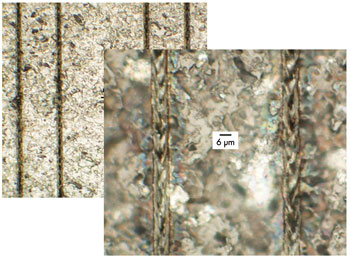
Figure 1. A top-view microscopy image reveals scribes on a sapphire wafer.
To determine the location of the “processing focal plane,”
test scribes were generated at various focal positions. These scribes were processed
using slow scan speeds to obtain more than 80 percent spatial pulse overlap. Figure
1 shows a top view of some example scribes. After the material was cleaved, an optical
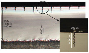
microscope was used to measure the cut depths. Figure 2 is a cross-sectional edge
view demonstrating scribe depths at various focal positions. The “processing
focal plane” corresponding to the deepest scribe was selected for conducting
the studies. With the theoretical spot size of 2.5 µm, groove widths achieved at
the “processing focal plane” during all of the experiments were 5 to
7 µm.

Figure 2. This cross-sectional edge view shows scribe depths corresponding to various focal planes.
For the sapphire wafers, an optical fluence between 30 and 400
J/cm2 was determined to be a good process window. If the applied laser fluence was
below the ablation threshold, no material was removed. At high fluence levels, however,
excess energy was wasted in heating the material. This material heating can cause
unwanted debris, cracking, melting and stress in the surrounding material, or what
is commonly referred to as “HAZ” (heat-affected zone).
Material removal thresholds are dependent also upon pulse duration.
Shorter-pulse-width lasers tend to have lower thresholds for material removal than
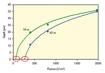
longer-pulse-width lasers. Figure 3 shows scribe depth at various fluence values
corresponding to 18- and 42-ns pulse widths. The data plot indicates that a clear
processing advantage exists with shorter pulse duration (18 ns) over longer pulse
duration (42 ns). Extrapolation of these logarithmic curves toward lower fluence
values clearly demonstrates that the material removal threshold with 18-ns pulse
duration is lower than that with 42-ns pulse duration. In addition, in the low fluence
regime close to 500 J/cm2, an 18-ns pulse duration results in deeper scribes compared
with those for 42-ns pulse duration. The data in Figure 3 indicates that with a
short-pulse-width laser, deeper scribes are achieved at low fluence levels, whereas
with a longer-pulse-width laser, more energy is needed to achieve the same depth.

Figure 3. A graph of scribe depth versus fluence charts the advantage of short pulse widths.
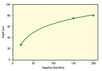
The benefit of operating lasers at high repetition rates to increase
throughput in laser processing is also well-known and is shown in Figure 4, where
scribe depth increases with increasing repetition rate. At the higher repetition
rates, the time between pulses is shorter and, thus, the thermal energy is deposited
in the material at a rate faster than energy is dispersed from the focal volume
by thermal diffusion. This facilitates increased heat accumulation at the focal
volume, resulting in localized heating and melting of the material, which leads
to increased material removal. Hence, for sapphire scribing, it is beneficial to
operate the laser at a low energy per pulse and at high repetition rates to take
full advantage of available laser energy for material removal.

Figure 4. A plot of scribe depth versus repetition rate demonstrates the advantage of a high repetition rate.
With the significant efficiency gain offered by LEDs over traditional
incandescent lighting, along with the movement toward energy conservation, the demand
for LEDs has exploded. And DPSS 355-nm Q-switched lasers provide an effective tool
for robust high-yield scribe-and-break wafer singulation processing for high-throughput
LED manufacturing. The DPSS UV lasers offer the shorter pulse width, higher repetition
rate and higher power needed to produce narrower and cleaner scribe lines at higher
speeds.
Meet the authors
All three authors work for Spectra-Physics, a division of Newport
Corp., in Santa Clara, Calif. Rajesh Patel is applications lab senior manager; e-mail:
[email protected]. Ashwini Tamhankar is senior laser applications engineer;
e-mail: ashwini.tamhankar@newport. com. Tim Edwards is a senior marketing manager;
e-mail: [email protected].