Reducing pixel size can increase a digital camera's performance. However, there are tradeoffs that need to be considered when going that route.
Albert Theuwissen, DALSA Professional Imaging
In the search for ever-higher pixel counts for the digital still camera, it is clear that, if chip size remains constant, then “more pixels” means “smaller pixels.”
The incentive in keeping the silicon area of the sensor as small as possible is lower chip cost. A larger chip also requires a larger and more costly lens, extra space on a printed circuit board and a larger camera body. Smaller pixels are the key to producing higher resolution sensors on the same silicon area — or to reducing chip size without affecting resolution.
Unfortunately, there are trade-offs. In this case, overall pixel performance. Whatever the technology used — interline-transfer, frame-transfer or full-frame CCD, or passive- or active-pixel CMOS — smaller pixels deteriorate performance.
Pixels as buckets
A pixel of a solid-state imager with its electron packet often is compared to a bucket of water. This analogy helps not only in understanding the working principle of the pixels, but also in explaining the influence of smaller pixels on imaging performance.
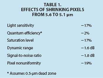
First, a bucket with a large opening can collect more water faster than a bucket with a small opening. The same is true for pixels: The light sensitivity, which is expressed as the amount of generated electrons per lux of incoming light, is directly proportional to the area of the pixels exposed to the incoming light. Changing the pixel size from 5.6 to 5.1 µm reduces light sensitivity by 17 percent.
 Every pixel in any type of sensor technology contains a kind of “dead zone” that is not light-sensitive. Mostly, this dead zone contains the isolation and separation structures between the pixels. Microlenses can counteract this loss in several technologies but never perfectly. Between two microlenses, for example, there is a dead space. Changing the pixel size from 5.6 to 5.1 µm in a technology with a 0.5-µm dead zone around the pixel — 0.25 µm accounted to every adjacent pixel — reduces the quantum efficiency by 2 percent.
Obviously, the maximum content of water in a small bucket is less than that of a large bucket. The same is true for imaging pixels. Very often, the whole area of a pixel cannot store charge. For example, only 90 percent of the area of frame-transfer, full-frame and passive-pixel sensor pixels can carry photogenerated charge. This figure drops to 50 percent in interline-transfer and to about 30 percent in active pixel sensors. This means that the saturation level deteriorates very quickly as the pixel area shrinks. Changing the pixel size from 5.6 to 5.1 µm will decrease the saturation level by 17 percent.
The dynamic range also varies directly with the saturation level; therefore, it will also shrink directly with the pixel area. Shrinking a pixel from 5.6 to 5.1 µm reduces dynamic range by 17 percent, or about 1.6 dB. It might seem that increasing the depth of the bucket will relieve the problem; unfortunately, this is not always possible for small pixels.
This statement about dynamic range is true when thermal noise determines the noise floor. In reality, this is not always the situation: At elevated temperatures or long integration times, dark current noise becomes dominant. The dependency of dark current noise on the shrinking pixel size is hard to predict. Smaller pixels can lead to a smaller dark current, but increased electrical fields in these pixels may produce dark current and its noise.

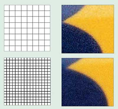
Figure 1. To keep digital still cameras small and inexpensive, designers look for small image sensors. To increase resolution without increasing sensor size, they shrink more pixels onto the same sensor area.
Assuming equal noise levels in two sizes of pixels, the one with the lowest light sensitivity or with the lowest quantum efficiency will generate the lowest signal-to-noise level. In a uniform illumination level across the total area of the sensor, the signal of the smaller pixel will be lower to the same degree as the decrease in product of light sensitivity and quantum efficiency.
Lowering the pixel pitch from 5.6 to 5.1 µm will drop the signal-to-noise ratio by 19 percent, or about 1.8 dB.
Pixel nonuniformities are caused by technological imperfections. These become relatively important if the pixel is designed with smaller dimensions. For example, the nonuniformity will be intensified by 19 percent if the pixel size shrinks from 5.6 to 5.1 µm.
New technologies
We can see that shrinking pixels to produce higher resolution from a given chip size goes hand in hand with major deterioration in pixel performance. It is worth noting, however, that pixel shrinkage usually occurs in parallel with other improvements in sensor technology. This means that the performance tradeoffs are valid only if the various pixels are made using the same technology.
Researchers are putting a lot of effort into improving the processing technology so that some of the negative aspects reported here are compensated by new technological developments, such as:
-
Increasing quantum efficiency by using optimized microlens shapes or microlenses composed of two components.
-
Increasing saturation levels by incorporating additional dopants during the production of the imagers.
-
Improving noise levels through technological steps and clever circuit design.
-
Switching to advanced processing techniques for silicon diffusion.
-
Using new camera lens designs to compensate for losses in sensor performance.
Regardless of these efforts, it is important to remember that, no matter what improvements can be made, the smaller the “bucket,” the less it can hold.