Jim Bovatsek, Jürgen Niederhofer and Dr. Rajesh S. Patel, Spectra-Physics
With a wide range of wavelengths, short pulse durations, high average powers and high pulse energies, compact and cost-effective diode-pumped solid-state (DPSS) lasers have a promising future in medical device manufacturing.
Medical device manufacturing is becoming more challenging every day as more functionality and features are added to the injectors, pumps, implants and other devices used to keep people healthy. There is a growing need for smaller devices with precise, high-quality, tiny features, and techniques beyond those found in traditional manufacturing are required to meet the challenge. Laser processing has been filling the need for quite some time; today, lasers are routinely used for marking, cutting and drilling of various materials during manufacturing of medical devices.
With almost anything related to human health, there are stringent requirements for materials and methods, and this is no less true for medical device manufacturing. The materials tend to be of high strength, purity and chemical resistance, often making them difficult to fabricate and process. They also run the gamut of material types – corrosion-resistant and high-strength metals such as stainless steel and titanium; high-strength ceramics such as zirconia and alumina; and an entire class of medical-grade polymers composed of various TPUs (thermoplastic polyurethanes), polycarbonates and fluoropolymers such as PTFE (Teflon). Not only must the materials be extremely pure, but manufacturing processes such as drilling and cutting must be as clean as possible – leaving behind minimal debris and residue – to minimize the need for costly and time-consuming postprocessing.
The laser marketplace for medical device manufacturing continues to be dominated by the high-average-power CO2 and the high-pulse-energy excimer. However, as devices (and, therefore, features) continually shrink and become increasingly specialized – which leads to lower production volumes – these lasers are proving to be unsuitable in some cases. Furthermore, with the high cost of ownership often associated with such lasers, medical device manufacturers are eager to find alternatives.
The performance of Q-switched diode-pumped solid-state lasers spans a large and growing range of powers, wavelengths and pulse durations, which is helpful in addressing the myriad materials used in medical devices. In addition, as this laser technology continues to advance, products are seeing significant improvement in the areas of packaging, upfront and ownership cost, ease of use, and – perhaps most important of all – reliability.
One example of a Q-switched DPSS laser system is the Spectra-Physics Explorer line, which includes 1064-, 532- and 355-/349-nm wavelengths at average power levels from 50 mW to 5 W – all within a narrow range of nanosecond pulse durations (~5 to 20) and in a compact design. Versions are optimized for (1) a low pulse repetition frequency (PRF) and high-pulse energy regime for the most difficult-to-machine materials – which is used in the first example below of catheter laser drilling – and (2) at lower pulse energies but higher PRFs, enabling fast execution of less energy-intensive processes – which is used in the second example below of laser marking medical devices.
Laser drilling for catheters
A common medical device manufacturing process that uses lasers is catheter hole-drilling and skiving, in which openings in catheter tubes are machined. These openings are used for venting, drug delivery and electrical wire conduit. Key requirements include little or no residual debris and very smooth edges to the features after laser processing is completed. Oftentimes, the tubing material is a polymer that may be difficult to machine cleanly. Materials such as silicone, Teflon, PEEK (polyetheretherketones) and TPUs such as Tecothane are commonly used. Required hole sizes range from 0.001 to 0.010 in. (25 to 250 µm), and tubing wall thicknesses are of similar dimension. For highest quality, lasers with UV wavelengths and short pulse durations are used.
Recently, Innovative Laser Technologies Inc. (ILT) of Minneapolis was contracted by one of its medical device customers to build a tool for machining such openings in polymer tubing. The system incorporated a 349-nm UV laser along with X-Y-Z motion, galvo-based beam delivery and automated machine vision for locating part features prior to drilling.
ILT had stringent requirements for processing quality, but the throughput target was achieved; the compact, capable system impressed team members, ILT project manager Jim Jacklen said. “Another great feature was the quick warm-up time. This allowed part processing to begin as soon as the system power-up was completed.”
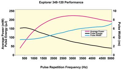
The short pulse widths and high pulse energy of this type of laser are well suited to cleanly machine these more difficult materials; at 500-Hz operation, it will deliver ~150 µJ of pulse energy with a 4-ns pulse duration (Figure 1). This translates into a high peak power (the ratio of the pulse energy to the pulse duration) of >35 kW. This is important because, for a fixed optical spot size, peak power and pulse energy can be primary determinants for whether or not a laser ablates a particular material. With the UV wavelength of 349 nm, many polymers will strongly absorb the laser light and will therefore be cleanly ablated by the laser.

Figure 1. The power, pulse energy and pulse duration of a typical Explorer 349 laser system. Q-switched diode-pumped solid-state lasers have a large and growing range of powers, wavelengths and pulse durations to address the various materials used in medical devices. Images courtesy of Spectra-Physics.
Even if the absorption is somewhat weak, however, a combined high energy and short pulse width means that material processing can still proceed without resorting to extremely tight focusing, which can be difficult to accomplish with common scanning galvanometer-based systems.
Laser simplicity and size also are important considerations for this application. ILT has been providing laser tools to the medical device industry for many years and is uniquely positioned to provide timely customized solutions. In this case, however, the end customer’s time line was too aggressive for a new tool design, necessitating instead that the laser be retrofitted into a larger, more typical workstation for medical device manufacturing.
“In order to meet a compressed project lead time, an existing system design was chosen that had been used with a different type of laser ablation process,” Jacklen said. That type of laser was significantly larger than the one selected, so the system could have had an even smaller footprint, he added.
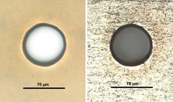
The tool and the laser are suitable for machining a variety of features in a variety of medical materials. In particular, the optical delivery system was designed with high-quality structuring of polymer tubing in mind. One such polymer is PEEK, a medical polymer with good mechanical strength and chemical resistance over wide-ranging temperatures. With proper process optimization, the laser machined clean holes in PEEK material with 0.003-in. (~80-µm) wall thickness (Figure 2).

Figure 2. Laser-drilled openings in smooth (left) and textured (right) surface PEEK polymer. With proper process optimization, the laser machined clean holes in the medical polymer.
The ablation of the polymer also had no apparent swelling or burring of the material at the edges of the holes, and very little residual debris was observed. Compressed air was applied during the process, but no cleaning or other postprocessing was performed on the features. Drilling time for each hole was ~100 ms.
Marking applications
Marking of medical devices is another large application space for lasers. Considering the wide range of materials and marking dimensions, a variety of DPSS laser systems can be of use for this application. In addition, many of these lasers are offered in high-PRF/low-pulse-energy configurations, allowing lower-energy pulses to arrive at rates of tens of thousands to more than 100,000/s for high-speed and “gentle” marking.
Of critical importance for this application is that the marking process remove as little material as possible because this will leave behind the lowest amount of debris contaminants. This implies that shorter-pulse-duration lasers are a good fit because there is shallower heating in the bulk of the material and, therefore, a lower likelihood of uncontrollable large-volume material removal. This prerequisite also means that a laser pulsing with lower energy but at a higher PRF will be advantageous from a process throughput point of view.
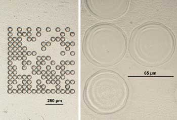
A common marking technique is a two-dimensional data matrix. For materials with strong absorption and a relatively low threshold for ablation, each dot in the data matrix can be realized with a single pulse. In Figure 3, the 2-D data matrix was generated on a medical polymer with a single-pulse-per-dot process. The relatively high pulse energy can be used to make fairly large matrix dots with just a single pulse – in this case, 65 µm in diameter.

Figure 3. Low- (left) and high- (right) magnification photos of 2-D data-matrix marking in medical polymer. This mark was generated with the Explorer 349 laser with a single-pulse-per-dot process.
Marking time for this type and size of feature is directly related to the laser’s PRF and the speed of the beam scanning equipment, and is typically in the range of tens to hundreds of milliseconds per matrix. It is important to note that, with such a single-pulse marking process applied over a small area (micromarking), a high laser PRF does not necessarily result in a faster process because the equipment for scanning the beam commonly cannot support more than a few kilohertz of laser pulsing frequency.
Larger medical implants, including those used for orthopedics, are fabricated with much harder materials, such as hard ceramics. Alumina (aluminum oxide, or Al2O3) has been used for decades in orthopedic implants such as hip replacements. In addition, thinner coatings of alumina can be applied to softer materials to impart higher strength to the components.
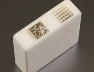
To create a 2-D data-matrix mark in alumina ceramic, a raster scan process was used in which each marked pixel in the matrix was composed of a group of closely spaced horizontal lines (Figure 4).

Figure 4. Fine-grain alumina ceramic marked with a 532-nm Explorer laser system. A raster scan process created a 2-D data-matrix mark in which each marked pixel comprised a group of closely spaced horizontal lines.
This material was marked with 1.5 W of power from a 532-nm laser system. The dimension of each filled pixel in the matrix is ~250 µm and was generated with ~30-µm raster spacing. Besides the data matrix marking, the photo also demonstrates the ability for gray-scale marking. In this case, variable contrast is achieved by changing the pulse energy (but with a fixed average power) and the beam scanning speed.
Medical device market outlook
Medical manufacturing is a growing industry that shows no signs of slowing. Physicians and other health professionals are increasingly teaming up with scientists and engineers to develop new technologies for enhancing and extending human life.
Recent market research indicates worldwide sales of medical devices at $300 billion in 2011.1 The US has the largest medical devices market, with estimated sales of roughly $105 billion in 2011.2
The aging population and the increases in cardiovascular diseases, diabetes, obesity and hypertension are the driving factors for the bigger medical device market in the US. Segments of the medical device industry include instruments used in cardiology, oncology, neurology, orthopedic, aesthetic and health care information systems. The drug delivery and implantable devices account for a large share of the market for medical devices.
All indicators suggest that medical device manufacturing will continue to be strong for lasers for years to come. Although excimer and CO2 lasers are a large majority of the market today, the trend toward smaller, more complex and more highly specialized medical devices is driving the need for simpler, high-performance laser solutions.
Meet the authors
Jim Bovatsek is applications laboratory manager at Spectra-Physics in Santa Clara, Calif.; email: [email protected]. Dr. Rajesh S. Patel is director of strategic marketing at the same branch; email: [email protected]. Jürgen Niederhofer is general manager at Spectra-Physics in Stahnsdorf, Germany; email: [email protected].
References
1. Zacks Investment Research, www.zacks.com/stock/news/50398/Medical+Devices+Industry+Outlook+%96+April+2011.
2. Espicom Business Intelligence, www.espicom.com/Prodcat2.nsf/Product_ID_Lookup/00000110?OpenDocument.