DAVID RASMUSSEN, PALOMAR TECHNOLOGIES ASSEMBLY SERVICES
David Rasmussen is general manager at Palomar Technologies Assembly Services and has more than 30 years of experience in the photonics and microelectronics industries. He holds two patents in the telecommunications industry.
The value of light-enabled products
and services is estimated to be between $7 and $10 trillion annually, which means the science of light represents roughly 13 percent of the world’s economy1. With the push toward smart cities, autonomous vehicles, and 5G, the demand for connected devices and higher-capacity networks is steadily growing, thereby increasing the need for light-enabled products and services, ushering photonics into a position of prominence in the world economy.
As the need for photonics-enabled
devices grows, so too does the need for core components. In 2016, more than 3300 companies were making photonic components2. To keep up with the demand and still remain profitable, these companies must continue to find methods to scale up volume, increase yield, and reduce costs in production.

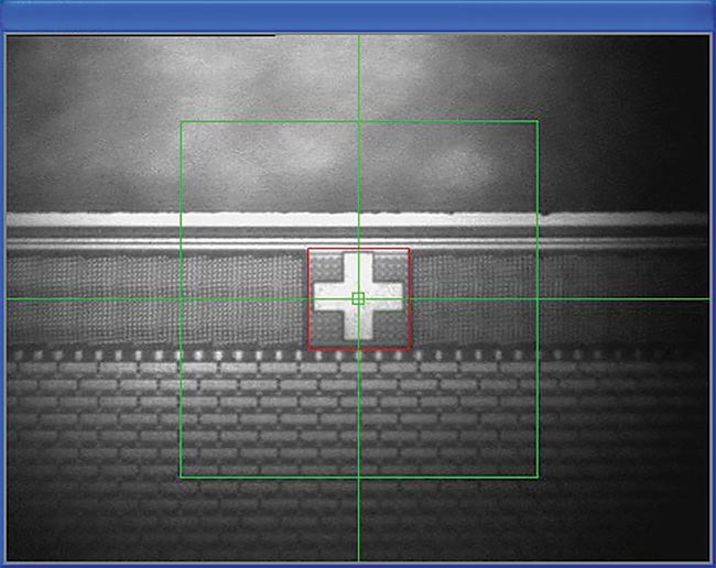
A clear, crisp cross fiducial is critical to optical component alignment. Fiducials that are difficult to see or find cost extra time and resources during the assembly phase. Courtesy of Palomar Technologies.
One way to face profitably challenges
is with a collaboration mindset. Developing a successful photonic device can involve diverse teams that are often large and composed of talented people who
may not understand one others’ roles — R&D scientists, design engineers, packaging engineers, manufacturing
engineers, and assembly technicians. They may not understand all the aspects of designing and manufacturing, and — to make communication even more difficult — they may be scattered around the country or the globe. A collaborative mindset can prevail.
When R&D scientists and design engineers possess a level of understanding of the nuances within the manufacturing process and equipment capabilities, key assembly challenges that affect yield and cost can be mitigated. In many R&D labs where photonic components are designed, there may be little understanding of the capabilities of die or wire bonding equipment, or the manufacturing processes that technicians employ to assemble photonics packaging.
A collaborative manufacturing process between R&D teams and an external contract manufacturer offers a means to successfully bridge the gaps in manufacturing experience that often lead to late
deliveries, high rejection rates of components, or increased costs due to design failures or changes. In a collaborative process, all critical areas of device design and manufacturing are brought together by the contract manufacturer into a process of continual feedback, enabling a more profitable project.
Collaboration at the start
While each project differs significantly,
the overall phases of collaborative manufacturing are the same. They include a definition of requirements, development and delivery of assembly drawings, and the requirements of processes such as material inspection, programming, manufacturing process development, prototype development, prototype feedback,
change requests, design freeze, and pilot
production. All of these happen before ramping up to either low- or high-volume production.
First, and perhaps most important, a successful collaboration requires that a full document package be created by the design team and the contract manufacturer. This enables them to jointly define and review component/package design and assembly requirements at the beginning of any project. In the package, they include agreements on the part quality, what to include in the assembly drawings, what materials are to be used, and how the final part will be inspected.
Clear assembly drawings that include datums and geometric tolerances relating to alignment requirements can improve communication between all team members, which ultimately can save valuable time and costs.
Optical manufacturing
For optics designers, one of the biggest areas where collaborative manufacturing
can have a positive impact is in fiducial design. Fiducials are markers or points of reference used to align components in the assembly process. Bad fiducials, such as those that are difficult to see or that are created in the wrong layer of the components, are a main reason for higher manufacturing costs. Appropriate fiducial location is critical to optical component alignment, so it is important to design repeatable, consistent fiducials relative to the optical features of the assemblies.
In addition, having a methodology to reference the parts appropriately increases efficiency and accuracy, broadens the
process window, and improves yield. Without these, time and cost to manufacture is significantly increased because time is spent troubleshooting process issues that are actually a result of the package design.
As with the assembly of optical components, fiducials are very important for the proper assembly alignment of dies to printed circuit boards (PCBs). It is important that fiducials are located on the active layer of the part. For example, on a PCB, fiducials must be placed on the copper layer of the package, rather than in the silkscreen layer. If the fiducials are not on the copper layer, the positioning accuracy will be compromised.
Other areas where collaboration can benefit understanding are in the final test requirements, in the need for traceability, and in how changes in suppliers or batches can affect costs and yield.
Working collaboratively with a company that has a deep understanding of
the equipment used in the manufacturing processes for optical and photonics package assembly can minimize the risks associated with any new product introduction.
References
1. National Research Council (2013). Optics and Photonics: Essential Technologies
for Our Nation. Washington, D.C.: The National Academies Press, https://doi.org/10.17226/13491.
2. SPIE: Optics and Photonics Industry Report 2019, http://spie.org/industry-resources/information/market-intelligence.