Advancements in the manufacturing of high-performance visible lasers hold the key to unlocking numerous application opportunities for quantum devices and throughout quantum science.
MARIE FREEBODY, CONTRIBUTING EDITOR
The visible range, spanning around 380 to 700 nm, has
longstanding use in photonics. Many materials have specific absorption, reflection, and transmission
characteristics in this band, which are exploited for applications from optical metrology and biomedicine to quantum and communications.
Increasingly stable and versatile visible lasers are populating the market, and the efficacy of these sources is intersecting with the emergence of chip-scale lasers — a burgeoning innovation area that is poised to benefit a range of disciplines. Chip-scale lasers promise to uniquely
address the need for small, low-power, and potentially low-cost sources.
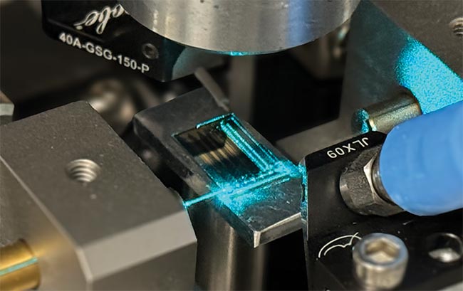
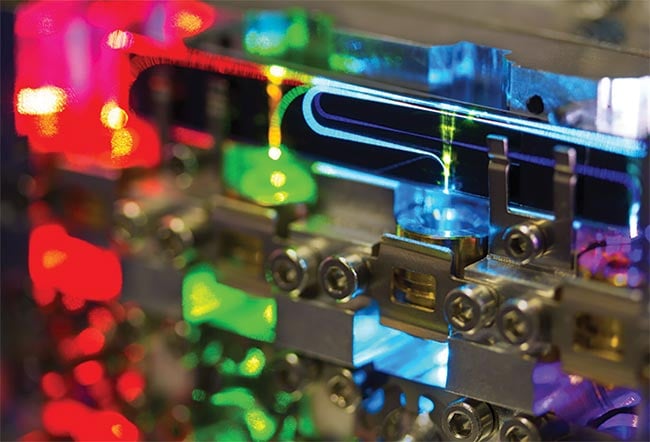
The combination of PIC hybrid integration technology and semiconductor packaging is critical to the transition of quantum operation from the controlled laboratory environment to commercial and industrial settings. Courtesy of Leonardo DRS Daylight Solutions.
In terms of both applied R&D and
productization, quantum devices, in
particular, are among the technologies
for which chip-scale lasing could serve as the catalyst for a wave of scientific and commercial progress.
Quantum comes calling
Because many of the physical systems used in quantum computing, communications, sensing, and metrology have optical transitions in the visible, as well as the near-infrared, visible sources are integral in quantum information science and technology (QIST). This includes neutral atoms and ions used in optical atomic clocks. With laser sources addressing optical transitions in the visible band, the potential use of neutral atoms and trapped ions spans applications that typically necessitate cooling, initialization, and state readout or the interrogation of specific transitions, said Stephan Ritter, director of quantum technology solutions at TOPTICA Photonics.
For example, trapped ion and neutral atom arrays are used in color center magnetometers as well as various types of quantum memories that are needed in quantum networks.
“For quantum computers, both neutral atom and ion-trap quantum computers use a number of visible lasers to establish, maintain, and control the qubits that form the base for quantum computation,” said Asger Jensen, senior market development manager and head of quantum photonics at NKT Photonics.
The advancement of on-chip lasing only heightens the application potential for visible sources. Integrating visible lasers in a chip-scale format, and particularly as part of PIC technology, could further enable advancements for quantum sensing, processing, and computing.
“The size, weight, power consumption, and cost (SWaP-C) scalability of PICs that operate in the visible are poised to enable what’s next in future quantum applications,” said Tim Day, senior vice president and general manager of Leonardo DRS Daylight Solutions.
“Along this road map, it is critical that stable, ruggedized lasers are incorporated into systems that are required to operate outside of the lab environment.”
Chip-scale visible lasers
The current proportion of the visible laser market pertaining to quantum application end uses is small in comparison to laser-commanding disciplines, such as spectroscopy, biology, and imaging. Dan Blumenthal, head of the Optical Communications and Atomic Quantum Photonic Integration Group at the University of California, Santa Barbara, estimates the market share to be around 10% to 15%.
This value is predicted to rapidly change — and at an uptick — given the pursuit of integrated, chip-scale quantum devices. The maturity of existing visible laser solutions, which are ready to support new-product design, reinforces such a forecast.
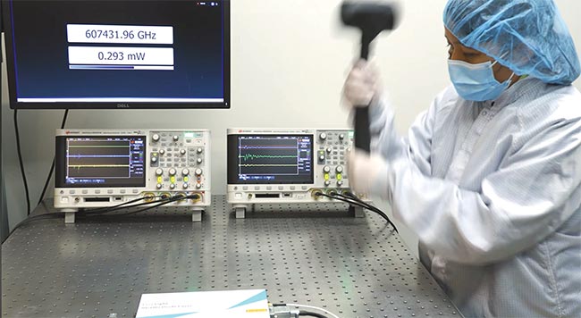
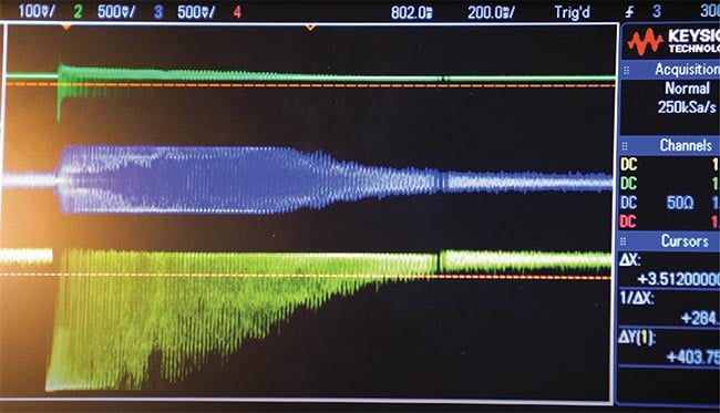
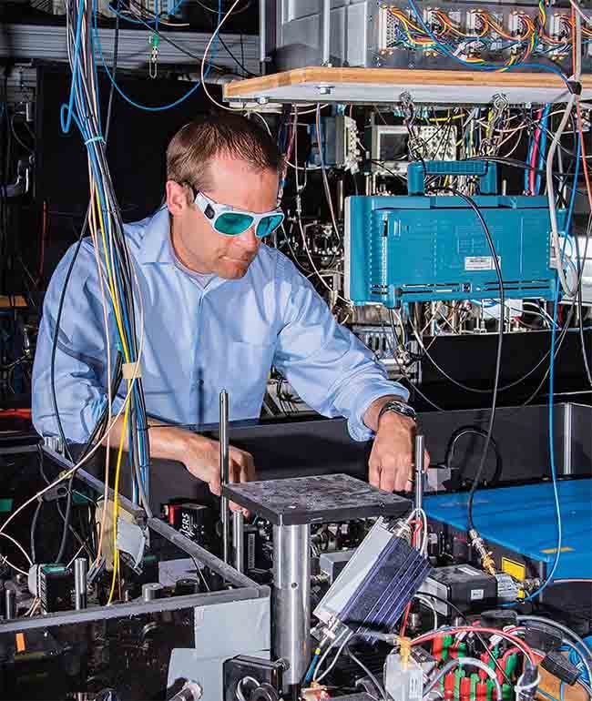
The commercial manufacture of visible lasers prioritizes ruggedization, among other qualities. One test involves pounding a table with a hammer (top) to ensure that the source stays in lock — indicating that it will maintain performance regardless of temperature or vibration extremes (bottom). Courtesy of Leonardo DRS Daylight Solutions.
“[Laser system developers] are still building tabletop lasers customized to each and every wavelength for quantum, and making money,” Blumenthal said. “There are expensive, brute force lasers for quantum, not reliable or inexpensive or compact. There is a realization that this has to change for quantum scale to become reliable.”
Blumenthal believes that quantum-
focused commercial entities understand the need for chip-scale visible sources and the need to be adaptable to the broad array of unique atomic and quantum wavelengths. For example, leading quantum information company Infleqtion acquired silicon photonics companies SiNoptiq Inc. (for which Blumenthal served as president and CEO) and Morton Photonics earlier this year. The acquisitions are intended to precisely address the emerging market for visible light integrated laser system technologies for quantum applications.
Manufacturers of quantum devices are not the only ones who recognize the current commercial opportunities. Laser manufacturers are increasingly aware of the commercial prospects in the quantum realm that could use integrated visible laser solutions.
“I have seen some laser makers that are putting a lot of resources into serving the quantum community, particularly on topics like clocks and quantum sensors that are a bit further along, though clearly quantum computing and communications are on their radar,” said Kartik Srinivasan, project leader and a fellow in the Photonics and Optomechanics Group at the National Institute of Standards and Technology (NIST).
In the commercial sector, NKT’s
Jensen echoes Srinivasan’s observation. He highlights the ongoing priority for laser manufacturers to support the road
maps of the laser-heavy quantum applications in platforms that are or will be viable for commercial use.
“These applications in quantum technology have in recent years seen a migration from labs into commercial ventures and a need to scale the systems, and as a consequence, the laser powers,” he said. “This has also facilitated a move from lab-appropriate laser technologies, such as titanium sapphire lasers chosen for their versatility, toward industrial laser platforms, such as fiber lasers.”
Quantum outside the lab
The challenges in transitioning quantum technologies for use outside of the laboratory are well stated for system developers all the way down the chain to system integrators. The difficulty in maintaining baseline, laboratory-level performance in real-world settings is a bottleneck that exists within this set of challenges.
According to Srinivasan, integrated lasers may unlock quantum applications by helping to make them deployable outside laboratory settings. However, they may not always provide strong benefits in terms of the absolute performance of the quantum technologies that they support. In some cases, he said, real-world performance may be worse than when using the very best laboratory laser technology. In essence, both the integrated laser and the quantum device system, as a result, may face drawbacks in performance when transitioning out of the laboratory.
This is not to say the transition is on hold.
“Leveraging the combination of semiconductor and PIC hybrid integration and packaging with product design rules that satisfy military environmental requirements makes a powerful combination when transitioning quantum operation outside of a controlled lab environment,” Day said. “Systems integrators across
the spectrum of quantum sensors, clocks, computers, and networking will need to consider ‘hands-free’ operation when deploying systems in real-world environments.”
Visible light PICs can be used for applications such as spectroscopy, metrology, and sensing. The PIX4life open access pilot line for PICs targets life sciences applications in the visible range. Courtesy of TOPTICA Photonics AG.
Amid the early stages of the shift to which NKT’s Jensen alludes, the majority of quantum applications that use visible lasers are in fundamental physics, quantum science and particle discovery, quantum sensing, optical atomic clocks, precision frequency metrology, and quantum computing. Typically, lasers and other photonic components are used to prepare the laser wavelength, phase noise, stability, amplitude, modulation, and detection for use in a quantum interrogating system in which the laser “touches” the atom, ion, or qubit. A move toward miniaturizing laser systems that are often bulky and expensive could reduce the cost of the quantum device. The likelihood of this cost reduction increases if the lasers are created through scalable fabrication processes.
Of the quantum applications that could be apt to emerge based on chip-scale lasers, Blumenthal puts quantum sensors and timekeeping first on the anticipated rollout timeline. Srinivasan agrees: He predicts that chip-scale lasers will make inroads into quantum sensor systems within a period of five years. Small, compact clusters of quantum processors and networking, followed by quantum computation, are applications that will likely come later, Blumenthal said. Because commercial quantum computers are not yet firmly established in the marketplace, there are other bottlenecks that must be overcome first.
“At the moment, companies are mostly focused on scaling up their processors in terms of the number of logical and physical qubits, and that’s what’s limiting now,” Srinivasan said. “Eventually, the laser size, weight, and power can be expected to be an issue, but advances in laser size, weight, and power must be such that laser quality (e.g., noise) is maintained, or else qubit quality may suffer.”
Applications that remain even more distant extend to space-based experiments, space-based quantum gravitational sensors, and global satellite navigation systems.
Integration demands
Without discounting the challenges
associated with advancing sophisticated technologies out of the laboratory and into industry, the physical challenge of integrating a visible source onto a chip remains a dynamic bottleneck in the visible sources/on-chip lasing discussion. This barrier is present beyond the realm of QIST.
It also extends beyond the design of the laser system.
“For the chip, you need to choose a material platform that is transparent in the visible wavelength range, like silicon nitride or aluminum oxide,” Ritter said. “Unfortunately, this is not the case for
indium phosphide, which is well established for applications at telecom wavelengths.” The distinct properties of different semiconductors and compounds are fundamental to photonic integration.
As such, this area of materials science is the source of widespread investigation in the R&D community, as well as in industry, given its influence on the development of chip-scale and integrated lasers.
In a 2022 research advancement, the Lipson Nanophotonics Group based at Columbia University demonstrated tunable and narrow linewidth chip-scale lasers for visible wavelengths shorter than red1. The group used micrometer-scale silicon nitride resonators and commercial Fabry-Pérot laser diodes in the work.
Critically, the researchers’ platform served to simultaneously minimize the material absorption and the surface scattering losses for all visible wavelengths.
Such dual minimization is typically a challenge of these architectures.
“If absorption is not an issue because of the choice of a suitable material, scattering losses due to edge roughness dominate,” Ritter said. “These losses increase strongly with the optical frequency and therefore put more stringent requirements on the fabrication process for visible laser sources compared to infrared lasers.”
Further, the smaller mode fields that are associated with the shorter wavelengths in the visible range require added precision in alignment and packaging, Ritter said. And, despite the dynamism that the combination of hybrid integration and packing present, hybrid integration of the semiconductor material with the optical chip, via edge coupling or heterogeneous integration, remains a difficult task to solve in systems using visible sources.
“All chip-based laser solutions require packaging techniques, which are less well established in the visible than in the infrared,” Ritter said.
“The on-chip integration of optical isolators to prevent reflected light from disturbing single-longitudinal-mode laser operation is an unsolved topic that requires more research.”
Though quantum applications are among those poised to benefit from continued progress in this aspect of photonic integration, they are not alone. The depth of applied research into the chip-scale integration of visible laser sources is also tied to end uses in AR/VR and high-performance displays.
Quantum leap
The growing emphasis on commercializing and deploying quantum technologies
corresponds to an ongoing shift in
emphasis to introduce new laser-specific requirements in SWaP-C. This focus on laser parameters intensifies the focus on system-level considerations, which are already prevalent.
Reliability, in the sense of where and how the laser can be controlled and coordinated with other lasers in a system, is one concern. An end user must be able to focus on an experiment by automating the application, without always needing “hands on” the lasers.
Another critical consideration is size and scale. Contemporary laser systems and their control mechanisms may occupy as much as 80% to 90% of lab- and rack-scale quantum infrastructure. This makes the current iteration of quantum devices expensive, power consuming, unreliable, costly, and in need of scaling.
Inherently, integrated lasers offer high potential for scalability for high-volume, low-power applications. Commonly, these sources are frequency-converted laser diodes.
But in terms of high powers, there is no way around fiber lasers due to their ability to dissipate excess heat. “When it comes to the most demanding power requirements, diode lasers in combination with fiber amplifiers are the best solution for many quantum technology applications,” Ritter said.
This feeds into another consideration: the variety of material systems that might be needed to enable access to optical gain and light emission across a broad range of wavelengths, including through the visible.
“There are so many choices of atomic and molecular species, it is the Wild West of lasers in terms of laser parameters, including wavelength and the coherence properties of the light,” Blumenthal said.
In the end, several different semiconductor laser gain media might be needed. How to best integrate those gain media with PICs will need to be determined.
Additional challenges remain. To fully realize the benefits of PICs from a lasers-first perspective, the PICs must be very low loss at the target laser wavelengths — a particular challenge at shorter wavelengths. There can also be more sensitivity to waveguide roughness, and wavelengths that are closer to absorption mechanisms in some PIC waveguide materials can limit the PIC’s optical power handling.
National Institute of Standards and Technology (NIST) physicist Andrew Ludlow and colleagues achieved atomic clock performance records in a comparison of two ytterbium optical lattice clocks. The photo shows the laser systems used in both clocks (foreground) and the main apparatus for one of the clocks (behind). Courtesy of NIST/Burrus via TOPTICA Photonics AG.
“Over the last couple of decades, different integration strategies have emerged at telecom wavelengths, both in order to integrate telecom gain media with PICs and to realize good laser performance, in terms of output power, tuning range, frequency noise, etc.,” Srinivasan said. “Some of these strategies are now being applied to visible wavelength lasers, and
I expect to continue to see significant
improvements in performance and integration in the coming years.”
Blumenthal suspects that science is on the verge of a transformation in quantum devices.
“We are on the cusp of transforming lasers, laser systems, and the optics and control needed for quantum to the chip scale, realizing a leap like that of computing in the 1960s,” he said.
Scaling up volume and investment
Although advancements in visible laser technology and quantum systems have historically occurred in parallel, certain underlying technical ingredients have influenced both technologies. For example, the demonstration of ultralow-loss PICs in the visible enables the design of very narrow linewidth and low frequency noise lasers. Low noise is critical for clocks and for high-fidelity qubit manipulation. At the same time, ultralow-loss PICs are useful for scaling up photonic quantum computation as well as for applications entirely outside of quantum and laser sources.
But as quantum applications develop a need for laser technology that is currently unavailable, the inverse also appears
evident. While the high level of investment in quantum technologies may present an attractive investment — from a commercial perspective — the quantum technologies road map remains unclear.
“Quantum technologies have a place in the future, without a doubt, but for now remain an insignificant part of the overall laser market,” Jensen said. “The large number of relevant laser variants combined with no single laser [that has been] used in quantum to reach a significant volume means it is yet to become as attractive from a commercial perspective as other laser applications.”
It is therefore important for other areas of the quantum community to continue to show progress in making their technologies more mature, so that laser developers can see that the quantum market is sustainable. Ultimately, sufficiently reliable, scalable, and cost-effective semiconductor laser diodes are compelling for many
applications. In particular, the scalability
of the underlying manufacturing processes of these lasers, as well as the ability to integrate them with other PICs technologies, makes them a commercially favorable technology.
Additionally, according to TOPTICA’s Ritter, the nature of the tie that binds
visible sources to quantum technologies is
such that a boon to one (quantum science or visible sources) is apt to directly
correlate to a boon for the other. Quantum technologies, he said, profit from new
visible laser sources, especially when they address commercially relevant aspects, such as SWaP-C, and provide a clear path toward scalability.
“Innovations in visible sources will, in return, find very promising and quickly growing markets in the vast field of quantum technologies,” Ritter said.
Also, it is critical to understand that distinct applications present different gauges of the significance and influence of forthcoming innovation.
“For quantum computers, scalability is essential to enable the very ambitious road maps regarding increasing the number of qubits. This requires power and reliability to increase, and size and cost to go down. In sensors, for example, some applications are only enabled by a very small footprint, while still others require stability over a broad range of environmental conditions.
“The interdependence between quantum technologies and laser sources has already proved to be beneficial for both fields, and I expect it to be an even stronger driver of innovation in the future,” Ritter said.
For laser manufacturers, the quantum
revolution, at least for the moment, could provide fertile ground to finance higher-risk laser developments that may otherwise have decreased in priority.
References
1. M. Corato-Zanarella et al. (2023). Widely tunable and narrow-linewidth chip-scale lasers from near-ultraviolet to near-infrared wavelengths. Nature Photonics, Vol. 17,
No. 2, pp. 157-164.