Dr Robert L. Byer and Dr. TomasPlettner, Stanford University
Might it be possible to combine today’s commercial laser technology with micro- and nanoscale manufacturing techniques to produce tabletop or even pocket-size particle accelerators? This has been the dream of many research groups around the world, including ours, and it’s a dream that is appearing more realistic every day.
High-energy electrons following a zigzag path are ideal for generating vacuum ultraviolet radiation and x-rays. Unfortunately, today’s sources of high-energy electrons are accelerators costing millions if not billions of dollars that are available to a very limited clientele of scientists.
In contrast, a compact tabletop laser-based electron accelerator could be the key to an inexpensive and short-wavelength source for the rest of us. Just as a fiber amplifier, for example, converts the photons from a diode pump into a collimated, high-brightness beam, a laser-based electron accelerator would convert the output of a laser into a beam of coherent, short-wavelength ultrafast optical pulses.
Electron beams with mega- to gigaelectron-volt energies are required to generate the wavelengths described in the previous paragraph, but even higher energies — perhaps in the teraelectron-volt range — might one day be achievable from laser-based accelerators. This would allow applications in the field of high-energy physics, where research currently is stymied by society’s inability to fund the multibillion-dollar price of bigger and bigger accelerators.
The laser accelerator technology that we are pursuing operates in a fashion similar to that of radio-frequency (RF) linear accelerators. The main difference is the choice of wavelength of the electromagnetic field that accelerates the particles, being reduced from centimeter waves for RF accelerators to micron wavelengths for a laser-driven particle accelerator. In essence, a linear accelerator is a structure that diffracts the laser or the RF wave such that it creates a force component that is parallel to the electron beam trajectory and that follows the electrons at the same velocity.
Thus, the electrons can be thought of as “surfing” an electromagnetic wave as they ride down the accelerator and as gaining energy if they are located on the correct phase of the wave. The choices for the material and the shape of the structure are therefore critical factors for generating the correct electromagnetic field configuration. Additionally, the accelerator structure should not interfere with the electron beam path. Finally, compact couplers that deliver the electromagnetic wave from the external source to the inside of the accelerator efficiently are essential for any accelerator.
In sum, linear accelerators could be thought of as a special class of diffraction structures, and the reader can appreciate immediately that feature size and the dimensions of the accelerator are proportional to the wavelength of the driving electromagnetic field. For a laser-driven particle accelerator, this is both a curse and a blessing. The small dimensions present a challenge in fabricating these accelerators and in determining the corresponding electron beam diagnostics and control elements that go with them.
The submicron features for most of these structures demand tolerances that cannot exceed a few dozen nanometers, which sets a serious constraint on the nanofabrication options, on the choice of materials and on the range of shapes that are possible to fabricate. Furthermore, the miniaturization of the dimensions drastically reduces the maximum electron bunch charge that these small accelerators can support — from the nominal nanocoulomb (109 electrons) of charge that is typical for RF accelerators to the femtocoulomb range (104 electrons).
On the other hand, the small dimensions of these devices do present a number of advantages. First, laser-driven particle accelerators feature a very small volume that must be filled with optical power, which is the main factor that allows the use of low-power megahertz-repetition-rate lasers for these accelerators instead of large petawatt-scale laser facilities. The high pulse repetition rate possible with low-power lasers circumvents noise from thermal cycles that plagues the larger low-repetition accelerator systems; thus, a smaller system presents a unique advantage in stability for applications that do not require large electron bunches. The short operating wavelength presents one final but crucial advantage over other acceleration technologies.
As described before, the electrons surf the electromagnetic wave that is traveling down the vacuum channel of the accelerator. When the laser field is adequately timed, the electrons experience a temporal focusing from the driving field and can form a bunch that occupies a very small fraction of the optical wave. In this fashion, a 1-μm-wavelength laser driving these accelerator structures could generate electron bunches with durations in the attosecond range. Although the bunches contain relatively few electrons, they still can produce high peak electron currents comparable to those of RF accelerators.
These attosecond timescale electron bunches can be directed into an undulator to generate coherent x-rays. The peak current from a laser accelerator is similar to that from a conventional accelerator, which requires tens of meters of conventional undulator structure to generate x-rays efficiently.
But what good is a pocket-size laser accelerator if such large undulators are needed downstream? In light of this, we and our collaborators at the advanced accelerator research department at the Stanford Linear Accelerator Center (SLAC) have proposed and are investigating a dielectric electron manipulation structure that functions in a fashion that is not too different from our laser-driven accelerator structures, except that it is tailored to provide a strong deflection force from the laser instead of an acceleration force. The proposed dielectric undulator can take advantage of the large peak forces available from lasers and, hence, can replace the conventional permanent-magnet undulators with a dielectric and monolithic device that is no longer than a pencil.
A wide range of geometries for laser-driven particle accelerator structures has been explored theoretically over the past three decades, but no experimental work had been carried out. In light of this, our group picked up on the theoretical developments and initiated an experimental program in the mid-1990s to demonstrate the key physics aspects for this particle acceleration technology. The experimental challenges associated with the short wavelength were indeed an obstacle; nonetheless, three years ago we succeeded in a first proof-of-principle experiment that demonstrated the following important properties: first, the linear dependence of the electron acceleration with the amplitude of the laser field; second, the need for an electric field component from the laser beam that is parallel to the electron trajectory; and third, the necessity for an adequate structure.
The successful experiment employed a single linearly polarized near-IR laser beam copropagating with a relativistic 30 MeV, 1-ps-long electron beam in the presence of a thin, disposable boundary. The interaction was characterized from the observed energy modulation of the electron beam and allowed for the verification of the key physics aspects mentioned before.

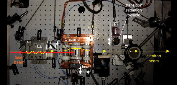
Figure 1. This photograph shows the setup employed in the microbunching experiment performed at SLAC. The laser and the electron beam trajectories are marked in red and yellow, respectively. The hole spacing of the breadboard is 1 in. IFEL = inverse free electron laser.
Surfing the optical field
The next key step was to demonstrate the ability of the particle acceleration process to form electron bunches that are substantially shorter than the laser wavelength and that can surf the optical field. Recently, we observed the formation of subfemtosecond electron microbunches. Figure 1 shows a schematic of the experimental setup. Verification of electron bunching was performed by observation of enhancement transition radiation at wavelengths that are harmonics of the driving laser field. So, now that subfemtosecond high-energy electron microbunches are available, we must show that we can preserve, or compress, the microbunches even further; we also must show that we can impart net energy to them with a second laser accelerator stage. This is our current experimental effort, which we expect to conclude in the next few months.
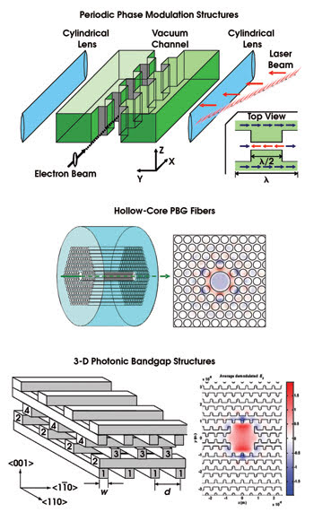
Our experiments have been aimed at demonstrating the key physics aspects and not at our ultimate objective of developing accelerator microstructures. Figure 2 illustrates three examples of microchip accelerator structures of interest to us — two are photonic waveguide designs, while the third relies on acceleration from periodic evanescent fields.

Figure 2. These three microstructure laser accelerators are being investigated at the Stanford Linear Accelerator Center (SLAC) and at Stanford University. In the near future, millimeter sections of these structures will be tested with an electron beam at SLAC.
Extensive theoretical work has already taken place, as have optical tests of some of these proposed structures, and our next objective is to begin testing the microstructures with an electron beam. They will be tested first in a passive form; passage of an electron beam through the accelerator structures causes them to radiate. The emitted radiation spectrum contains valuable information on how best to couple the laser beam to the accelerator structure and on how well it performs as an accelerator when powered by the laser beam. Hence, the first tests of these structures with an electron beam will include the characterization of the radiation pattern from millimeter-long sections of the structure.
The next set of experiments will aim at observing particle acceleration from these millimeter-long sections when they are powered by a laser. The ultimate objective in this research phase will be demonstrating gradients in the hundreds of MeV/m to ~1 GeV/m and demonstrating retention and manipulation of the subfemtosecond electron bunches in the microchip structures. Finally, cascading of subsequent millimeter-length sections will prove important in showing the concept of linear acceleration and also will provide the first lessons for developing an extended microstructure accelerator.
An intermediate objective is a centimeter-long structure that could deliver a beam of several MeV. Such a “pocket size” prototype structure could itself be an interesting tool for ultrafast electron microscopy and, depending on the electron beam energy, could be valuable for direct pump-probe experiments.
A similar research and development path is envisioned for developing the laser-driven dielectric deflection structures. We are designing an experiment to test a single millimeter-long dielectric laser-driven deflector structure. This will be followed by an experimental effort where we learn how to cascade the deflector elements until we accomplish a dielectric-based undulator structure — a key element for our envisioned tabletop attosecond radiation source.
Meet the authors
Robert L. Byer is a professor in the applied physics department at Stanford University; e-mail: [email protected].
Tomas Plettner is a research associate in the applied physics department at Stanford University; e-mail: [email protected].
Our collaborators at SLAC work in the advanced accelerator research department under the direction of Robert H. Siemann.