CCD device allows for fast results in solar cell quality measurements.
Dr. Gerhard Holst, PCO AG
As a result of the world’s climate situation and the rising cost of fuel, “clean” methods of energy generation are drawing considerable interest. The result has been a significant boom in solar cell manufacturing over the past few years.
Solar cells are large-area semiconductor devices with typical dimensions of 15.6 cm. Loss mechanisms such as locally reduced diffusion lengths or parallel resistances often curtail the energy conversion efficiency of solar cells. Characterization techniques that can provide spatially resolved information about the performance of a solar cell therefore are important to manufacturers not only in research and development but also in solar cell production, in which capacity the methods serve as process control tools.
Unfortunately for manufacturers, most of the current characterization techniques for spatially resolved information are time-consuming because the image must be generated from point-by-point measurements. Recently, Takashi Fuyuki and his colleagues at Nara Institute of Science and Technology in Ikoma, Japan, introduced a camera-based electroluminescence imaging technique that allows for rapid solar cell characterization at high spatial resolution.1

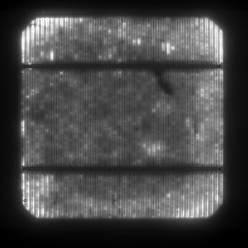
Figure 1. Shown is an image of a monocrystalline solar cell operated under forward bias condition. The electroluminescence of the cell below the bus bar and the grid electrodes is clearly visible. The image was recorded with a solar model CCD camera system at 2-s exposure time. The darker areas in the image indicate regions of minor quality within the solar cell.
Based on his paper, the Institut für Solarenergieforschung Hameln in Emmerthal, Germany, used the sensicam qe, a cooled CCD camera manufactured by PCO AG of Kelheim, Germany, with an IR operating mode to set up this technique and to investigate its potential for solar cell characterization.2
Because this technique does not dictate the distance between the camera and the solar cell, solar cells and panels of any size can be analyzed. A more detailed analysis of particular areas with higher spatial resolutions can be achieved easily by reducing the distance between the camera and sample and by selecting the appropriate lens. A meaningful image can be captured in a couple of seconds. The measured electro-luminescence is the emission of light resulting from a forward bias voltage applied to the solar cell. The electrons injected into the solar cell recombine with the available holes by transferring their excess energy to an emitted photon. The intensity of the luminescence radiation is determined by the product of the electron and hole concentrations. In simple terms, the product of the electron and hole concentration increases exponentially with the externally applied bias voltage.
The image captured with the CCD camera shows the intensity distribution of the luminescence radiation. Although a homogeneous distribution would be expected for an ideal solar cell, electroluminescence images of actual solar cells always show inhomogeneities. Even though the reasons for such a local reduction in the carrier concentration can be numerous, they can be distinguished clearly in most cases. Thus, local variations in the bulk-carrier lifetime — such as those in multicrystalline silicon — are clearly visible on the electroluminescence image.
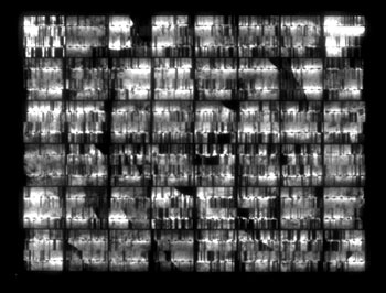
Figure 2 clearly shows the impact of too much pressure when applying the grid electrodes, as all the dark fingerlike structures and black areas show that the solar panel is damaged at these locations. Previously, solar cell investigations were performed with either single-point and scanning measurements or with IR thermal cameras, with their disadvantages of lower spatial resolution and higher costs.

Figure 2. This image of a solar cell panel shows a variety of areas that are destroyed or that are not operating properly. Vertical dark lines represent cracks, a consequence of high mechanical tension that occurred when the grid electrodes were applied. Dark corners suggest broken areas in the solar cells. Not all dark areas will contribute to solar current generation.
With the special low-light/NIR-operation-mode technology integrated into the CCD camera, images were recorded at 1- to 2-s exposure times, with a resolution of 1392 × 1040 pixels. The increased quantum efficiency of the camera that uses the ICX285AL interline-transfer CCD sensor was achieved by an improved bias and timing control. Besides gaining experience with the sensicam qe, we optimized and improved the NIR performance within the design of the pco.1300 solar camera. Although this camera is not as deeply cooled as the other, more detailed quantum efficiency measurements revealed that this quality, as with physics state, can be an advantage for this application.
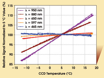
Figure 3 shows the normalized signal of the solar camera when the CCD is operated at various temperatures. For VIS applications, there is a slight increase of signal at higher versus lower temperatures, but for the NIR, the graph clearly shows an increase of signal for higher temperatures. To exploit this phenomenon, a low-noise CCD image sensor was required because noise and dark current increase with temperature. A binned high-resolution CCD sensor, on the other hand, is not always an advantage because it tends to have high noise figures, which are not changed by the binning.

Figure 3. This graph depicts signal curves of a solar model CCD camera system operated at various temperatures of the CCD image sensor and illuminated with light at various wavelengths. The signal was normalized to the value at 5 °C because the light sources delivered a range of intensities.
Therefore, both the special NIR operation technology and the thermoelectric cooling at temperatures in the range of 5 to 15 °C, together with an extreme offset stability (offset drift <1 count per hour), favored the solar camera to achieve camera-based electroluminescence measurements. This enabled the depiction of the impact of various loss mechanisms in solar cells with high spatial resolution and within very short measurement times.
In summary, this characterization technique has become an important tool in research and development and has contributed to promoting investigations in the fields of wafer-based cell development and of the integrated module assembly of silicon thin-film solar cells.
Meet the author
Dr. Gerhard Holst is head of the science and research department at PCO AG in Kelheim, Germany; e-mail: [email protected].
References
1. T. Fuyuki et al (June 2005). Photographic surveying of minority carrier diffusion length in polycrystalline silicon solar cells by electroluminescence. APPL PHYS LETT, June 24, 2005, Vol. 86, 262108.
2. K. Bothe et al (April 2006). Electroluminescence imaging as an in-line characterisation tool for solar cell production. 21st European Photovoltaic Solar Energy Conference, Dresden, Germany.