Feats of engineering are enabling atomic force microscopes to do amazing things on Earth and on Mars.
The Phoenix Mars Lander has scoured the surface of the red planet’s Arctic circle for signs of life. On July 9, the robot took the first atomic force microscope (AFM) image ever recorded on another planet.
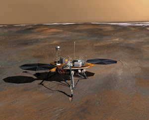
The Lander as it would look on Mars. The Lander has cameras, a meteorological weather station with a laser, a mass spectrometer, a calorimeter and an optical microscope, in addition to the first AFM to go to Mars. Courtesy of NASA Jet Propulsion Laboratory at CalTech.
A consortium in Switzerland built the first AFM robust enough to operate on Mars. The consortium included the University of Basel, the University of Neuchatel and Nanosurf AG, a Liestal-based company that manufactures AFMs.
To understand why the scientists designed the AFM the way that they did, it is important to understand the way AFMs work. These microscopes construct images by feeling the surface with a cantilever that has a tip so fine that it can’t be seen with the naked eye or even with a regular light microscope. The tips can have diameters of less than 5 nm. One nanometer is just 1/100,000 of the width of a sheet of paper.
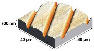
The first AFM image ever taken on Mars is of Martian soil. The 40 × 40-μm area is so small that it fits on an eyelash. The grooves are 300 nm deep and 14 μm apart. The vertical dimension in the image is exaggerated for emphasis. Courtesy of NASA Jet Propulsion Laboratory at CalTech.
In many cases, AFMs have a laser beam focused constantly on the cantilever. The laser beam is aligned so that it bounces off the cantilever and into a photodetector. As the cantilever moves on the surface of a sample, the cantilever’s movement causes the laser beam to hit a different point on the photodetector than it did before, and a computer program can use those points to construct an image.
“Aligning a laser beam to the end of a cantilever is not very easy on Mars,” said the leader of the project, Urs Staufer, who recently left the University of Neuchatel to chair a department at Delft University of Technology in the Netherlands.
Instead of a laser, the researchers used piezoresistors to sense the cantilever movement. Piezoresistors are materials that generate resistance to an electrical current that can be measured in response to mechanical stress. Similarly, the piezoelectric effect is the ability of certain materials to generate electricity in response to mechanical stress or to move in response to electricity.
The fine scanning motion of the cantilever is often controlled with piezoelectric ceramics, but the researchers wanted a larger range of motion than ceramics would allow. Although larger piezoelectric materials and high voltages would increase the scanning area, neither of those options would work well on Mars.
So they devised an electromagnetic system using permanent magnets and voice coils. The system is smaller than a matchbox, yet it can generate deflections up to 60 μm.
It’s lonely out in space
Because no one is on Mars to change the cantilever tips when they break, wear down or become contaminated, the scanner contains eight cantilevers on a single sensor chip.
“Breaking off the used cantilever was probably the most precise manipulation ever conducted on another planet so far,” Staufer said. The team aligned the cantilever with the precision of a few microns and then broke the cantilever without touching or otherwise compromising the next cantilever, which was less than 100 μm away. The system, with its ability to move up and down in increments of less than 1 μm, also moved precisely to a position where it could measure the sample.
“The AFM proved to be astonishingly robust,” Staufer said. “There were, of course, some hiccups but no real serious problems.” Namely, the heat from the stepper motors that moved the microscope and the large temperature variation on the planet caused the AFM measurements to drift, which was not good because measuring temperature was not part of the scientific procedure.
The scientists used the AFM to observe Martian dust and soil particles. They observed rounded and platelike particles, among other shapes, and they found particles less than 1 μm in diameter. In contrast, the optical microscope on the Phoenix Mars Lander can resolve objects 4 μm or larger. “The AFM delivers … images in a completely new size domain to the planetologist,” Staufer said.

The Phoenix Mars Lander has been investigating the Martian Arctic circle for signs that the red planet supports or once supported life. Courtesy of NASA Jet Propulsion Laboratory at CalTech.
Measurements by the mass spectrometer and other devices on the Phoenix Mars Lander have shown that the Martian soil includes clay and calcium carbonate, the main component of chalk. Because most carbonates and clays form only in the presence of liquid water, these experiments provide evidence of the presence of water on Mars. The Lander conclusively found ice below the surface of the soil, and a meteorological laser system on the Lander detected falling snow. The presence of liquid water would indicate that the Martian environment has been favorable for life.
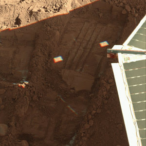
The Lander dug in this area and found ice under the Martian surface. Courtesy of NASA Jet Propulsion Laboratory at CalTech.
The entire Phoenix Mars Lander project was the result of a collaboration of many people. Professor Peter H. Smith at the University of Arizona in Tucson has the distinction of being the first university researcher to lead the investigative aspect of a Mars mission. Along with Smith, people from other universities and institutions designed and built the various measurement systems on the Lander; for example, the Swiss consortium designed and built the AFM.
Lockheed Martin Space Systems in Denver designed and built the Lander itself, and NASA’s Jet Propulsion Laboratory at the California Institute of Technology in Pasadena managed the journey of the Lander to Mars and its return to Earth. More information is available at www.nasa.gov.
Project Millipede
Here on Earth, researchers led by Mark Lantz at IBM in Rüschlikon, Switzerland, have been developing AFM systems to store and read data in mobile phones. They recently completed development of a new prototype of such a system.
At the same IBM laboratory, Gerd Binnig and Heinrich Rohrer developed the precursor to the AFM, the scanning tunneling microscope (STM), for which they won the Nobel Prize in 1986. In that same year, Binnig announced with Christoph Gerber and Calvin Quate the development of the first AFM.
“I think this sort of history of development of AFM and STM has given us a strong tradition,” Lantz said. “It developed into a strong interest in nanotechnology.” He sought and accepted a position at IBM because, in his words, “I was impressed by the quality of work that comes out of what is really a small research lab here, both in the basic sciences and in the applied areas.”
Lantz’s current project, to develop AFM systems for mobile phones, has been going on for more than 10 years. At IBM, the project is known as “Millipede.” Using a single AFM, he and his colleagues have written data at maximum rates of about 100 Mb per second and have read data at maximum rates of about 100 kb per second, assuming that one bit is equivalent to one symbol or indentation written by the AFM. “It’s very slow still compared to a hard disk drive or flash memory,” Lantz said.
To increase the data rate, Lantz’s latest prototype uses hundreds of thousands of cantilevers. The fine motion of the cantilevers is controlled using voice coils and permanent magnets, as with the AFM that went to Mars.
Lantz said that the data rate of this system is theoretically faster, but the researchers have not yet tested it. They are concentrating instead on measuring other properties, such as storage density.
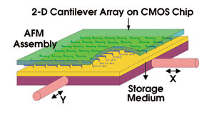
Researchers at IBM in Switzerland developed an array of AFM cantilevers that writes directly to a polymer surface. They plan to use this system to store and read data in mobile phones. Reprinted with permission of IBM Journal of Research & Development.
Underneath a CMOS wafer, the cantilevers read and write directly to the surface of a polymer. The system stores data by making indentations in the polymer, and it reads the data by scanning those indentations. The researchers have been using poly-aryl-ether ketones as the polymer.
The researchers also heated the polymer while making and reading the indentations because heating makes the polymer more malleable. Heating also reduces the friction and, consequentially, the rate at which the cantilever tips wear down.
While writing data, the cantilever is heated to 400 °C by means of a heater integrated directly above the tip. After the cantilever stops writing, the heat and pressure from the AFM are turned off, and the indentation stays in the polymer. During reading, a second heater near the tip is heated in the range of 150 to 300 °C.
The researchers demonstrated that they could use the system to store 840 Gb of data per square inch. They believe that the system has the potential to store more than 1 terabit per square inch. They detail this work in the July/September issue of the IBM Journal of Research & Development.
This research could have other applications as well. AFMs can create patterns of recessed areas in the surface of semiconductor wafers so that the transistors or other electronic configurations can be built in those recessed areas. And AFM is already routinely used to inspect CMOS wafers in production lines.
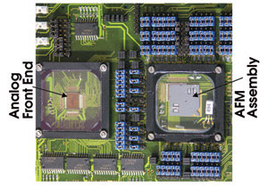
The AFM assembly fits on a circuit board. The assembly is controlled with a personal computer, which sends signals to the analog front end. The front end is the electronic interface on the circuit board that the IBM researchers can use to control the AFM assembly. Analog denotes that the front end is analog as opposed to digital. Reprinted with permission of IBM Journal of Research & Development.
Because there is a strong trend toward decreasing the size of the semiconductor wafer transistors for computer processing, eventually those wafers will be so small that details on them will not be able to be seen with anything but AFM. “AFM is the only technology with sufficient resolution to do the job, but [AFMs] suffer from this limitation that they’re inherently slow,” Lantz said.
In addition to increasing the speed of AFMs, the researchers have been experimenting with various materials to try to prevent the cantilever tips from wearing down. They have found that silicon tips provide the greatest storage densities, but they wear down more quickly than desired. The researchers can coat the tips, but coatings can make the tips dull and thus decrease the resolution of their measurements. So far, tips molded from silicon-doped diamondlike carbon have provided the best trade-off between robustness and precision.
Lantz said that AFM cantilevers in commercial applications will have to be able to scan continuously for tens of kilometers without the tips wearing down. Otherwise, commercial devices using AFMs will break down and need service frequently. Naturally, most consumers lack the knowledge and equipment to replace the cantilevers. Tip wear depends on many factors, including the applied force, the material being scanned, and the presence or absence of moisture.
Only commercial applications have the problem of tip wear because scientists with the expertise and equipment can change cantilevers regularly without much hassle. Cantilevers are also relatively cheap.
Although scientists still face many engineering problems to make AFMs into more widely used devices, they already have developed a new prototype of an AFM system for mobile phones and for the first AFM system to land on Mars. Besides these materials science applications, AFM is being used frequently in biology and may be a medical tool someday. The future looks bright for this tiny tool.