Refractive index is modulated by optically exciting free carriers.
Breck Hitz
Optical switching — in which one beam of light modulates, or switches, another — is one of the holy grails of modern photonics. It’s a necessary technology for optical computing and for “transparent” optical networks, where optical information is transferred from one location to another without conversion to electronic form.
Different approaches to optical switching have been pursued in many laboratories around the world, but, recently, researchers at the Institute for Atomic and Molecular Physics in Amsterdam, the Netherlands, and at the University of Minnesota in Minneapolis, demonstrated, for what they believe is the first time, optical switching based on modulating the bandgap in a 3-D photonic crystal.

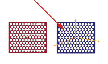
Figure 1. Spontaneous emission of an atom embedded in a silicon 3-D photonic crystal is inhibited if the crystal’s bandgap corresponds to the photon’s energy (left). However, an incident laser pulse can excite free carriers in the silicon via two-photon absorption, changing its refractive index and, therefore, the crystal’s bandgap. With the bandgap no longer the same as the atom’s energy, spontaneous emission can occur (right). Images reprinted with permission of the Journal of Applied Physics.
The bandgap in a photonic crystal is a wavelength range in which light cannot propagate because the crystal’s periodicity allows only standing electromagnetic waves at those wavelengths. The physics of a photonic bandgap in a photonic crystal is exactly analogous to that of an electronic bandgap in a semiconductor.

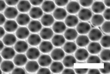
Figure 2. The researchers fabricated an inverse opal photonic crystal by infusing an opal crystal with silicon, then etching out the opal with hydrofluoric acid. The white scale bar in the photograph is 2 μm.
The recent result is especially exciting because modulating the bandgap of a photonic crystal opens possibilities beyond “mere” optical switching. For example, the spontaneous emission of an atom embedded in such a crystal could be controlled. If the crystal’s bandgap corresponded to the atom’s emission wavelength, emission would be inhibited (Figure 1, left). If an incident laser pulse quickly changed the bandgap, the atom no longer would be inhibited and could emit spontaneously (Figure 1, right).
In their demonstration, the scientists fabricated an inverse opal photonic crystal of polycrystalline silicon (Figure 2). Rather than attempting to inhibit spontaneous emission — shown in Figure 1 — they were content in this initial experiment simply to demonstrate a shift in the photonic bandgap.

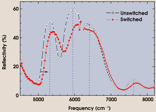
Figure 3. The reflection spectrum of the photonic crystal between 2 μm (5000 cm–1) and 1.43 μm (7000 cm–1) showed a clear shift to shorter wavelengths (red trace) after the pump pulse was incident upon the crystal.
They used a laser probe to measure the crystal’s spectral reflectivity before and after they directed a pump pulse into the crystal. The pump pulse and the probe were generated by a pair of optical parametric amplifiers from Light Conversion Ltd. of Vilnius, Lithuania, that were pumped by a Ti:sapphire laser from Spectra-Physics of Mountain View, Calif. The parametric amplifiers were tunable between 470 nm and 2.6 μm and produced 150-fs pulses containing more than 20 μJ.
The spectral reflection, as monitored by the probe beam, showed an unambiguous shift to shorter wavelengths as a result of the pump beam (Figure 3). Each of the three stop-bands of the photonic crystal — indicated by the vertical broken lines in Figure 3 — was shifted. The scientists believe that this shift indicates that the crystal is suitable for controlling the directional propagation of light.

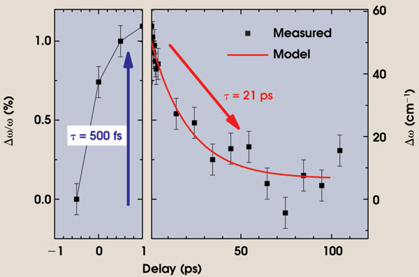
Figure 4. The rise time of the bandgap shift was faster than the fall time and was limited by the duration of the pump pulses.
By varying the delay time between the pump and probe pulses, they measured the speed of the bandgap’s shift (Figure 4). The ~500-fs rise time was limited by the duration of the pump pulses and was faster than the ~21-ps fall time. Even so, the fall time is much faster than the decay time of free carriers in bulk silicon — because the inverse opal crystal was polycrystalline silicon — and the grain boundaries are efficient carrier recombination traps. The fast response shown in Figure 4 led the investigators to propose that gigahertz switching speeds are possible with this technique.
Journal of Applied Physics, Sept. 1, 2007,053111.