Agilent Funds GA Tech Center
ATLANTA, Oct. 5, 2007 -- The Georgia Institute of Technology announced yesterday that has received $13 million from test and measurement company Agilent Technologies Inc. to establish a new electronic design automation simulation center at the university's Georgia Electronic Design Center in Atlanta.
Under the agreement, Agilent will supply electronic design automation (EDA) software, support and training to the new center, to be called the Agilent EDA Simulation Center. The center will provide radio frequency (RF) and microwave system and circuit design instruction and additional software design capabilities to Georgia Tech students, and licenses at no cost or at greatly discounted rates to startups in wireless communications design at the Georgia Electronic Design Center (GEDC).

The Georgia Electronic Design Center is broadly focused on fostering technology at the intersection of today’s communications applications: wireless/RF, wired/copper and fiber channels.
“This is one of the largest academic donations of Agilent EEsof products to a single institution to date,” said Jim McGillivary, vice president and general manager with Agilent’s EEsof EDA division. “We realize that universities and startup incubator programs play a crucial role in pushing the limits of EDA tools.”
“We are excited about Agilent’s participation with us. The company’s EDA tools help us continue to advance the technology and support our students, as well as to encourage and support commercial innovation,” said Joy Laskar, director of the GEDC and Schlumberger Chair in Microelectronics in the Georgia Tech School of Electrical and Computer Engineering (ECE). “We also want to contribute to the success of other academic and nonprofit institutions through sharing our experience in this partnership with Agilent, and we are making plans to release large portions of work using the Agilent EEsof EDA platforms for academic use.”

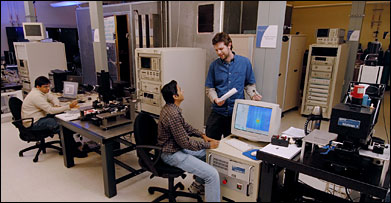
Researchers work in the high-frequency lab at the Georgia Electronic Design Center (GEDC).
The university said the deal significantly expands its longstanding relationship with Agilent and is a key part of the company's strategy to develop extensive relationships with key universities worldwide through the newly created Agilent EEsof EDA University Alliance program, which provides three-year custom licenses of Agilent EEsof EDA tools to startups.
The venture, located at Georgia Tech’s Technology Square, is expected to be fully operational by year’s end.
For more information, visit: www.gatech.edu
/Buyers_Guide/Agilent_Technologies_Inc/c421