Rostislav Rokitski, R. Rafac, R. Dubi, J. Thornes, J. melchior, T. Cacouris, M. Haviland and D. Brown, Cymer Inc.
A new flexible 90- to 120-W ArFi excimer laser system enables high-volume multiple-patterning manufacturing as well as 450-mm wafer applications.
Demand for increased semiconductor device performance at low cost continues to drive the shrinking of the feature geometry on silicon wafers. Over the past decade, argon fluoride (ArF) excimer laser systems operating at 193 nm and producing high output power have played a key role in patterning the most advanced features for high-volume deep-ultraviolet (DUV) lithography.
Lithographic patterning has progressed from ArF dry to ArF immersion (ArFi) to double- and multiple-patterning applications, with increasingly tight requirements for the quality of light at 193 nm and improved system reliability. This drove the transition from single-chamber laser systems to dual-chamber systems with ring cavity amplifier architectures.
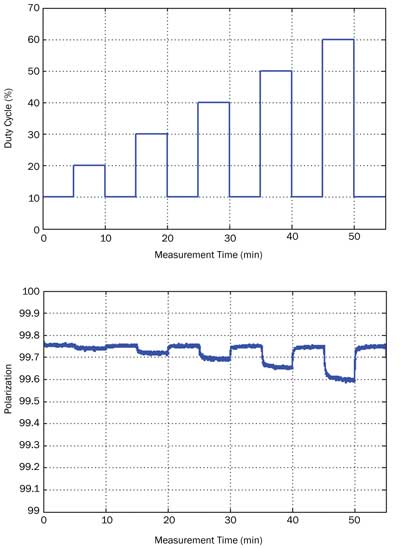
Figure 1. 120-W laser system duty cycle and output beam polarization, measured at 6-kHz, 20-mJ output pulse energy.
Since their introduction in 2007, XLR laser systems with ring cavity amplifier architecture have demonstrated flexibility and high reliability under diverse operating conditions for lithographic patterning applications.1 The range of applications extends from ArF dry to multipatterning immersion lithography, including high-dose applications and those with enhanced depth of focus for contact hole patterning.2,3
Advancing deep-ultraviolet lithography to 2x/1xnm nodes and reducing costs have driven increased wafer-stage scanning speed and transition to 450-mm wafer size. This transition requires additional power from the light source and a larger range of system duty cycles. It imposes tighter requirements on system stability as the number of pulses within an exposure window is reduced. System reliability and availability under this more stringent and challenging set of operating conditions are expected to meet or exceed the levels demonstrated by 60-W and 90-W laser systems in high-volume manufacturing environments.3
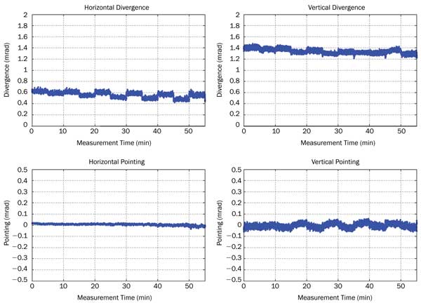
Figure 2. Far-field performance parameters of the 120-W laser system, operating at 6 kHz, 10 to 60 percent duty cycle.
A flexible 90- to 120-W light source will enable these future high-volume DUV lithography applications. Based on the flexible 60- to 90-W architecture of the previous generation, the technique delivers improved performance to meet the requirements for high-dose applications and to support the transition to 450-mm wafer size. The system output power, operating wavelength and spectral bandwidth can be varied in a wide range for each wafer, providing flexible system operation under diverse conditions.
Technology for 120-W operation
Excimer laser systems employed in the semiconductor industry for high-volume manufacturing produce light in the form of pulses, with pulse duration in the 60- to 150-ns range and typical energy of 5 to 20 mJ per pulse. The combined energy of multiple pulses delivered per unit area of semiconductor wafer is used for photoresist exposure. Light sources with 60- and 90-W output power produce pulses with 10- and 15-mJ nominal energy, respectively. The laser’s higher output power is achievable either by increasing pulse repetition rate or by increasing the energy of every pulse. In the laser system design described here, 120-W output power is achieved by increasing nominal pulse energy from 10-15 mJ to 15-20 mJ while maintaining the range of pulse repetition rates.
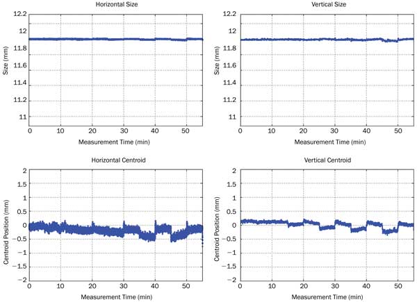
Figure 3. Near-field performance parameters of the 120-W laser system, operating at 6 kHz, 10 to 60 percent duty cycle.
Development of powerful and reliable 193-nm light sources historically represented a significant technological challenge. The vast majority of the commonly used optical materials degrade under exposure to high-peak-fluence 193-nm light. Calcium fluoride (CaF2) typically is used for transmissive elements inside the light source. Despite its relative robustness when compared with other optical materials, the surface and bulk of CaF2 are damaged under continuous exposure, typical for uninterrupted operation in a high-volume semiconductor manufacturing environment. This damage to optical component material ultimately limits module lifetime and can have a negative effect on the light source’s mean time between the interrupts, increasing the cost of ownership.
Compared to beam delivery, illumination and projection lithographic systems, the risk of material damage is significantly higher inside the excimer light source due to the high peak fluence of the optical beam. Optical components inside the light source are subject to significantly higher optical power of the beam, with substantially shorter pulse duration and beam size. Damage to CaF2 components can occur in bulk material via calcium colloid formation4 and on the surface through calcium fluoride conversion to calcium carbonate.5 These damage mechanisms are being addressed by material and component manufacturers to support long component lifetimes at elevated pulse energies.
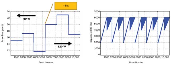
Figure 4. Light source operating conditions during a performance stress test with fast power switching. Nominal power is switched from 90 to 120 W during the test, simulating a wafer/lot exchange.
In addition to optical material damage due to increased pulse energy, thermally induced lensing and birefringence effects can be observed at elevated power load on the light source’s optical components. These phenomena can cause variation of beam polarization as well as near- and far-field profile with the laser duty cycle. With tight performance requirements under all operating conditions, thermally induced birefringence and thermal lensing must be addressed by increasing the output power level to 120 W. The 120-W light source addresses these potential issues with a combination of optical and mechanical component improvement as well as optical material selection for extended lifetime. The outcome of this effort is reduced sensitivity of output beam parameters to operating duty cycle (Figures 1-3).
Stability of all near- and far-field parameters of the output beam and polarization is very important for maintaining stable illumination conditions during wafer exposure. Beam parameter performance of the system, operating at 20-mJ output pulse energy and 6-kHz pulse repetition rate, was evaluated at various duty cycles (Figure 1). Output polarization stayed in a narrow range of 99.5 to 99.8 percent at all duty cycles, showing no significant effects of thermally induced birefringence. Far- and near-field parameters of the output beam show little dependence on the duty cycle of the system, indicating its stable performance. Low dependence of the beam parameters on output power level (Figures 1-3) ensures minimal contribution of the light source to wafer illumination.
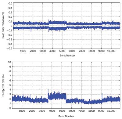
Figure 5. Dose and energy stability performance of the laser system at 90- and 120-W nominal output power settings during the stress test. STD = standard deviation.
Fast power switching
The system achieves fast power switching between 90 and 120 W by using intracavity attenuating elements to modulate losses in the ring power amplifier. This approach allows the master oscillator subsystem of the light source to operate under the same conditions at 90 and 120 W, reducing disturbances on output performance parameters associated with the master oscillator. The power ring amplifier gain element operates under the same conditions at 90 and 120 W as well, resulting in fewer transient effects when the dose is changed significantly between wafers or lots of wafers.
To evaluate the system’s performance under various operating conditions and output power levels, we performed a stress test, where the output pulse energy is varied in the range of 11.6 to 23 mJ, and pulse repetition rate is changed between 1500 and 6000 Hz. These test conditions cover the majority of cases observed during high-volume manufacturing.
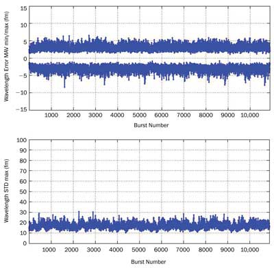
Figure 6. Wavelength stability performance of the laser system at 90- and 120-W nominal output power settings during the stress test. MAV = moving average.
In addition to the near- and far-field parameters of the beam contributing to illumination conditions, the following also can directly impact dose, focus and critical dimension uniformity performance: energy, wavelength and spectral bandwidth. As scanner stage speed increases, requirements on stability of these parameters are tighter, as fewer pulses are used to expose the unit area on a wafer. The XLR 600ix laser systems historically demonstrated stability of dose, wavelength and spectral purity. At increased output power and reduced integration window size, this performance level is maintained under all operating conditions.
Excellent dose stability with reduced integration window size, as seen in Figure 5, satisfies the performance requirements of the lithographic tools under all pulse repetition rates and energy settings. No significant dependence of energy stability on the output power range setting was observed.
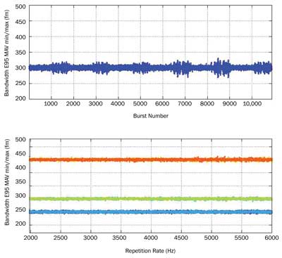
Figure 7. E95 stability performance of the laser system at 90- and 120-W nominal output power settings during the stress tests.
The focus stability of the image projected on the wafer can be affected by variation in the wavelength via chromatic aberrations in the scanner’s projection optics. To support stable focus, the light source must maintain wavelength stability within a tight range under all operating conditions, including different power settings and repetition rates. Figure 6 shows that the wavelength stability of the 120-W light source remains undisturbed with nominal power and energy target settings.
E95 is another important parameter affecting uniformity of critical dimension of the features etched on semiconductor wafers, defined as the spectral width of the source’s output light that carries 95 percent of the beam’s total energy. The results of the stress test described above – as well as repetition rate tests in a wide range of energy and E95 targets – demonstrate E95 stability in a wide bandwidth range (Figure 7), supporting critical dimension uniformity matching between different lithographic tools.
Meet the authors
Rostislav Rokitski is a principal systems engineer at Cymer Inc. in San Diego; email: [email protected]. Co-authors Robert Rafac, Ricardo Dubi, Joshua Thornes, John Melchior, Theodore Cacouris, Mary Haviland and Daniel Brown also work at Cymer.
References
1. D.J.W. Brown et al (March 27, 2007). XLR 500i: recirculating ring ArF light source for immersion lithography. Proc SPIE, Vol. 6520, Optical Microlithography XX.
2. R. Rokitski et al (March 16, 2009). Enabling high volume manufacturing of double patterning immersion lithography with the XLR 600ix ArF light source. Proc SPIE, Vol. 7274, Optical Microlithography XXII.
3. T. Cacouris et al (2012). Advanced light source technologies that enable high-volume manufacturing of DUV lithography extensions. Proc SPIE, Vol. 8326, Optical Microlithography XXV.
4. U. Natura et al (Dec. 29, 2009). Study of haze in 193nm high dose irradiated CaF2 crystals. Proc SPIE, Vol. 7504.
5. M. Bauer et al (May 11, 2009). Exterior surface damage of calcium fluoride outcoupling mirrors for DUV lasers. Opt Expr, p. 8253.