100K Dpi Printing Unveiled
ZURICH, Switzerland, Sept. 11, 2007 -- A new technique allows the printing of particles as small as 60 nanometers -- roughly 100 times smaller than a human red blood cell -- in complex patterns at a resolution of 100,000 dots per inch. The level of control offered by the nanoprinting technique could lead to breakthroughs in nanoscale biosensors, ultratiny lenses inside future optical chips, and the fabrication of nanowires for next-generation computer chips.
Scientists in IBM's Zurich research lab, working in collaboration with those from ETH Zurich (the Swiss Federal Institute of Technology), demonstrated the new, efficient and precise technique to "print" at the nanoscale by recreating Robert Fludd's 17th century drawing of the sun (the alchemists' symbol for gold) using 20,000 gold particles that were all 60 nanometers (nm) in diameter (the width of a human hair is approximately 80,000 nm) and printing them onto a silicon wafer.

This image created by IBM scientists demonstrates a new nanoprinting technique they believe will lead to breakthroughs in ultratiny chips, optics, and biosensors. The recreation of Robert Fludd's 17th century drawing of the sun was made by precisely placing 20,000 gold particles, each about 60 nanometers in diameter, or 100 times smaller than a human red blood cell. The technique translates to a resolution of 100,000 dots per inch (dpi), compared to offset printing's standard of 1500 dpi. (Images courtesy IBM)
The technique translates to a resolution of 100,000 dots per inch (dpi), compared to the 1500 dpi common in offset printing today, IBM said, and represents the smallest piece of artwork ever printed from single-pigment particles.
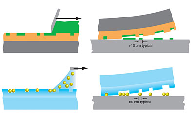
"In traditional gravure printing, a doctor blade is used to fill the recessed features of a printing plate with ink, in which pigment particles are randomly dispersed," said Tobias Kraus of the nanopatterning team in Zurich. "In our high-resolution printing, a directed self-assembly process controls the arrangement of nanoparticles on the printing plate or template. The entire assembly is then printed onto a target surface, whereby the particle positions are precisely retained at a resolution that is three orders of magnitude higher than in conventional printing."
Although still a few years from being used widely, the researchers said the new technique could lead to high-volume manufacturing techniques for nanostructures inside chips and other devices that are more efficient and cost less than today's methods because it allows scientists to place individual particles precisely where they want them.
"This method opens up new ways to precisely and efficiently position various kinds of nanoparticles on different surfaces, a prerequisite for exploiting the unique properties of such nanoparticles and for making their use economically feasible," said Heiko Wolf, researcher in nanopatterning at IBM's Zurich lab.
The work, published in the September issue of the journal Nature Nanotechnology, offers a new tool for use in a wide range of fields and industries such as biomedicine, electronics and information technology that seek ways to exploit the often unique properties of nanoparticles, which are defined as particles smaller than 100 nm.
Until now, standard top-down microfabrication techniques produce such tiny particles by in effect carving them out of a bigger piece of material, IBM said. Printing, in contrast, adds ready-made nanoparticles onto a surface in a very efficient way and allows for different types of materials such as metals, polymers, semiconductors, and oxides to be combined in one process.
The printing process could be used in biomedicine to print large arrays of beads that can identify certain cells in the body from supertiny samples to rapidly screen for cancer cells or heart attack markers, IBM said.

Top: The traditional printing method known as "gravure printing," where an image is etched on the surface of a metal plate, the etched area is filled with ink, then the plate is rotated on a cylinder that transfers the image to paper or other material. This method allows for features as small as 10,000 nm, far too big for use in electronics. Bottom: IBM's new nanoprinting method, which uses a self-assembly process to control the arrangement of tiny nanoparticles, in this case 20,000 gold particles, each about 60 nm in diameter. The gold nanoparticles are swept across a surface and convective forces in the liquid push the particles into grooves in the surface, forming nanostructures with a well-defined geometry.
Nanoparticles can also interact with light. With the new method, optical materials with new properties could be printed for use in optoelectronic devices. So-called "metamaterials" could be created in which the printed structures are as small as the wavelength of the light and therefore act as if they were a single lens with unusual properties, according to IBM.
The method also holds promise for semiconductors. In one experiment, the researchers achieved the controlled placement of catalytic seed particles for growing semiconducting nanowires, which are promising candidates for future transistors in microchips.
The printing template geometries explored include lines to produce closely-packed nanoparticle wires, which could be used in molecular electronics; regularly spaced arrays of gold particles as seeds for nanowire growth; and arbitrary arrangements, such as the printed replica of the sun. The long-range accuracy, which measures the deviation from the desired arrangement on a large area, is similar to that of microcontact printing methods, IBM said.
The next steps will be to refine the method to achieve even higher accuracies, as would be required for large-scale integration in microelectronics, as well as to extend the method to print even smaller particles.
For more information, visit: www.ibm.com
Published: September 2007