Techspec Fused Silica Wafers
Edmund Optics Inc.Request Info
BARRINGTON, N.J., July 25, 2014 — 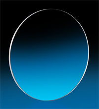 With less than 10-Å surface roughness, Techspec Fused Silica Wafers from Edmund Optics can be used as test substrates for measuring optical coating quality.
The thin, circular pieces of UV-fused silica provide 40-20 surface quality with RoHS compliancy. All wafers have thicknesses of 1 mm and a transmission range of 0.2 to 2.2 µm.
Techspec wafers are ultrasonically cleaned and can also be used in semiconductor microlithography, micro-electrical-optical applications or set-up processes as dummy components.
https://www.edmundoptics.com
/Buyers_Guide/Edmund_Optics_Inc/c4064
Published: July 2014
REQUEST INFO ABOUT THIS PRODUCT
* First Name:
* Last Name:
* Email Address:
* Company:
* Country:
Message:
When you click "Send Request", we will record and send your personal contact information to Edmund Optics Inc. by email so they may respond directly. You also agree that Photonics Media may contact you with information related to this inquiry, and that you have read and accept our
Privacy Policy and
Terms and Conditions of Use.
Register or login to auto-populate this form:
Login
Register
* Required