Photodiode Arrays
Hamamatsu CorporationRequest Info
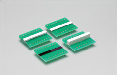
BRIDGEWATER, N.J., July 29, 2011 — For x-ray inspection applications, Hamamatsu Corp. has released the S11212 and S11299 series back-illuminated silicon photodiode arrays. They offer high-sensitivity uniformity across the array, as well as a robust structure. The 16-element arrays are designed with minimal variations in sensitivity between photodiode elements as well as at the sensor’s edges. The improved uniformity provides optimal x-ray images.
 The back surface for coupling to the scintillator has no bonding wires or photosensitive areas, so there is less risk of damaging the photodiode array, and the output terminals are bump-bonded to the board instead of being conncted with fragile wires.
The S11212 has a package size of 25.4 × 20 mm, while the S11299’s package size is 25.4 × 10.2 mm. Both are supplied in several scintillator configurations. Sensors coupled with CsI(Tl), GOS ceramic or phosphor sheet scintillators are available. A bare-chip sensor without a scintillator is also available for those who prefer using their own.
Multiple arrays can be tiled to create a long and narrow detector for x-ray inspection. As another option, two arrays can be layered for dual-energy x-ray imaging.
https://www.hamamatsu.com
/Buyers_Guide/Hamamatsu_Corporation/c5841
Published: July 2011
REQUEST INFO ABOUT THIS PRODUCT
* First Name:
* Last Name:
* Email Address:
* Company:
* Country:
Message:
When you click "Send Request", we will record and send your personal contact information to Hamamatsu Corporation by email so they may respond directly. You also agree that Photonics Media may contact you with information related to this inquiry, and that you have read and accept our
Privacy Policy and
Terms and Conditions of Use.
Register or login to auto-populate this form:
Login
Register
* Required