Short-wave infrared (SWIR) imaging with InGaAs-based cameras is well suited to nondestructive identification of materials, their composition, coatings, and other characteristics.
Sensors Unlimited Inc., A Collins Aerospace company
Imaging has long been used in industrial processes to measure, monitor, control, or otherwise manage the production of goods. The challenge to the process designer is to develop a tool that captures vivid and measurable contrast of the monitored objects’ characteristics. The shortwave infrared band provides that contrast in a variety of processes, ranging from agricultural products like foods and textiles, to chemical products such as pharmaceuticals and packaged goods, to hot industrial processes including glass and metal manufacturing.
Moisture strongly absorbs in the SWIR, which enables users to check coatings or bulk material dryness uniformity or check fill levels inside opaque packaging while ignoring printed graphics that confuse the eye. Hot processes for glass bottles, steel rolling, and metal smelting use SWIR cameras to remotely monitor temperature, uniformity, critical dimensions, and process end point. Maintenance inspections of furnaces used for chemical recovery, incineration or energy generation are performed by SWIR cameras, helping to keep processes running at full efficiency. The SWIR thermal-imaging applications also benefit from using commonly available, low-cost and easily replaceable glass lenses and windows, in contrast to germanium and silicon lenses used with mid- and longwave thermal cameras.
Many times, SWIR can “see” through coatings that are opaque to the eye. This enables visualization of underlying features such as fill levels, anticounterfeiting security codes or hidden moisture while using the same standard glass optics used by other machine vision cameras.
A variety of imaging and illumination techniques are available to help users adapt SWIR imaging to their measurement needs, whether they be stationary, moving on a conveyor belt, or in a continuous process stream. Line-scan (1D) and area (2D) cameras can be used to view the scene directly with lenses, filters, or spectrometers and to capture chemical composition or uniformity data. Hyperspectral images or datacubes, consisting of 3D datasets of spectra at each X and Y coordinate in a scene, are acquired by using tunable filters on lenses or by using imaging spectrographs in front of a 2D camera. These hyperspectral imaging systems multiply the power of real-time, online process control systems to control quality characteristics on multiple products simultaneously, ensuring product repeatability and throughput while reducing waste and rework.
What is the SWIR?
Shortwave infrared is generally defined as the band of wavelengths of light beyond that which is visible to the eye out to the limit where glass “cuts off” or absorbs, rather than transmits, the light. This encompasses the wavelengths of 0.7 to 2.5 µm. This range is also known as the near-infrared (NIR), but some associate this term with the band from 0.7 to 1.1 µm because of the upper limit of the working range of silicon detectors like CCDs and CMOS imagers.
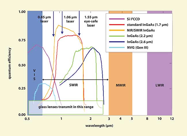
Figure 1. The electro-optical spectrum shows the relationship of the visible, shortwave infrared, midwave infrared, and longwave infrared wavelength bands. Also illustrated are the response curves for detectors in the visible and shortwave IR.
Indeed, others, working with cryogenically cooled compound detector materials like mercury cadmium telluride (HgCdTe, aka MCT) or indium antimonide (InSb), define the SWIR band as running from 1 to 3 µm. However, an alternate compound semiconductor detector technology, indium gallium arsenide (In(x)Ga(x-1)As) responds to much of that range with the power and cost advantage of room temperature operation. Most industrial applications are well served by the standard detectors covering the 0.9 to 1.7 µm range and use the ratio of 53% indium to 47% gallium (In0.53Ga0.47As), which matches the crystal lattice constant of the detector substrate material, indium phosphide (InP). By varying the indium-to-gallium ratio to In0.82Ga0.18As and using moderate cooling, 1D detectors with response out to the glass lens cut-off of 2.5 µm provide lower cost and higher responsivity than other technologies. Further, by thinning the substrate of the lattice-matched 2D detectors, cameras that simultaneously image the visible and SWIR range (0.4 to 1.7 µm) are available. This allows a single detector to see features of objects only seen in the visible as well as phenomenology only viewable in the SWIR, e.g., through coatings or underlying structures inside silicon integrated circuits (ICs).
As shown in Figure 1, a graph of the electro-optical spectrum, visible wavelengths are generally defined as spanning 0.4 to 0.7 µm, mid IR (MWIR) spans 3 to 5 µm and longwave IR (LWIR) runs from 7 to 14 µm.
Spectroscopic analytic techniques
For industrial processing of materials and products, the wavelength bands below 5 µm are important because of the unique spectral absorbance of reflected light at specific wavelengths caused by the motion of molecular bonds in materials at frequencies corresponding to light frequencies, or the interaction of the photons with the energy state of atoms.
By combining filters or wavelength dispersive optics with detectors, the resulting chemical signature of many materials can be determined remotely. With careful calibration, the proportion of these different materials can also be quantified. While the fundamental molecular wavelength bands are in the mid-IR and absorbance signatures are the strongest there, detectors are poor, requiring cooling to cryogenic temperatures to achieve significant signal-to-noise ratios. However, molecular absorbance is also evident at shorter wavelengths in the SWIR and visible wavelengths, where the detectors have better signal-to-noise performance. Another SWIR advantage is the variety of off-the-shelf photographic lenses available to optimize the inspection field of view at the standoff distance required by the process. Mid-IR equipment requires custom lenses and windows made with expensive materials.
Some examples of analytical techniques used to detect and recognize molecular chemical signatures are FTIR/FT-NIR, Raman spectroscopy, and diffuse reflectance NIR spectroscopy. The first two are largely confined to scientific or quality control labs and rarely make it out to the industrial process line. They generally require taking a sample from the production line and placing it in a test vial, and then placing it in a test fixture. The FT techniques use a moving mirror to create interferograms, which are disturbed by the vibrations typically present on the shop floor. Raman typically requires high-power lasers and long detector integration times in order to have enough signal for a good spectrum.
Both FTIR and Raman instruments can be used on real-time processes by using fiber optics to relay the signal to the instrument, but this restricts the measurement to sampling a spot. In contrast, reflectance near-IR spectroscopy with focal plane arrays permits checking the uniformity over a wide area.
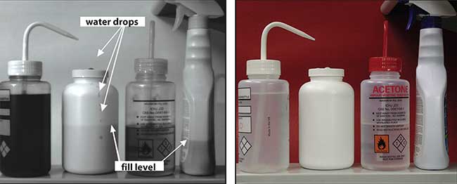
Figure 2. SWIR image (left) shows InGaAs technology’s ability to see the levels in plastic bottles, even those opaque to the eye. Contents from left to right: water, water, acetone, and a cleaning agent. Note that the water droplets on the outside of the pharmaceutical bottle are clearly visible in the SWIR image.
NIR spectroscopy works remotely very well to identify materials from molecular absorbance of reflected light as objects pass by on a conveyor belt or line. InGaAs cameras typically operate arrays at room temperature, enabling compact, low-power cameras compatible with the factory floor. By setting up the illumination to shine on the sample from many angles, the reflectance signal picked up by the detector(s) is dominated by the underlying bulk material instead of just by the surface of the material under test. This technique is known as diffuse reflectance. It avoids surface (or specular) reflections, which tend to carry chemical information about just the first few microns of the surface. The resulting short path length yields minimal absorbance that is difficult to detect, especially if the detector is swamped by the mirrorlike reflectance of many surface finishes.
With diffuse reflectance, the surface reflections into the detector are minimized and averaged with light that has interacted with many molecules in the bulk of the material, thus increasing the wavelength-dependent absorbance. Figure 2, a photo of a white pharmaceutical bottle illustrates this. In the SWIR image on the left, the water level is clearly evident as liquid water strongly absorbs in several bands, with peaks at wavelengths of 1.19 µm, 1.45 µm, and 1.94 µm. Less light is reflected to the detector through the walls of the plastic where the liquid has absorbed it. These wavelength bands are also used to determine water concentration or dryness level in many industrial material or coating processes. This further illustrates major advantages of near-IR spectroscopy for industrial process monitoring as little or no sample preparation is needed and remote sensing is relatively easy.
Integral to near-IR spectroscopy is a technique known as chemometrics, where spectra are taken of test samples with different concentration levels of the materials to be monitored. Software can be trained to recognize the key wavelengths to be used in determining the concentration levels in unknown samples. Process engineers must ensure that the training set includes all variations and measurement conditions, and that the calibration doesn’t drift over time, but the method has proved invaluable for industrial process control.
The detectors used for these spectroscopy techniques include single photodiodes, linear arrays of photodiodes, or 2D matrix arrays. These are combined with single wavelength filters, tunable filters, spectrometers, or imaging spectrometers, a lens or fiber optic, and a computer to make the system complete. An alternative to using filters is to use one or several monochromatic light sources. Increased availability of bright LEDs at a variety of wavelengths in the SWIR band is enabling system integrators to simplify the design and lower costs. LEDs permit switching wavelengths far faster than tunable filters of rotating filter wheels, without tuning artifacts, optical distortion or motion blur. Thus, a system with a single camera imaging alternate frames of 1300 and 1450 nm illumination would be able to use the ratio of two frames to monitor moisture uniformity while normalizing out common reflections in both frames.
Choosing the best combination of detector, light source, and wavelength depends on the application, the number of spectral wavelengths required to identify the chemistry, along with the dimensions, quantity, and speed of the products being monitored. Simple cases may be served with only one or two detectors behind wavelength filters to sample a coating on a moving web of product. When uniformity is needed, a linear array behind a filter can image the whole width of the web.
Adding additional array/filter combinations enables measuring the concentration of a material and/or detecting contaminants. However, if multiple wavelengths and uniformity are needed, then imaging spectrometers coupled with 2D arrays permit capturing multiple spectra at many points across the image. If the object being monitored is moving, or the lens image is swept across the imaging spectrometer input slit by a mirror, a 3D dataset is created in a method called hyperspectral imaging. An alternate hyperspectral method is to use a tunable filter in front of a matrix camera, recording complete images at different wavelengths to build the 3D hyperspectral cube. Either method provides the system flexibility to work with a variety of industrial processes or even constantly changing processes.
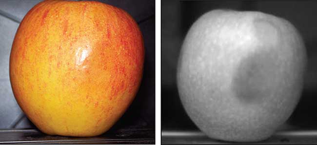
Figure 3. SWIR image (right) shows bruises that are hidden by the natural coloring of the apple.
Hyperspectral systems are often a good investment as process development tools. Working with chemometric software, they will identify the one, two, or three key wavelengths that can be used to monitor the critical process characteristic. Then the system integrator and process engineer can use a simpler system of a fixed filter and detector or line-scan camera for each key wavelength, reducing the data storage and processing time requirements and increasing throughput.
Some application examples are:
- Agricultural processors are using combinations of line cameras in the SWIR and in the visible, each with a different filter, to detect contaminates, such as packing materials, mixed in the incoming raw material arriving via conveyor belt.
- Detection of dents or bruises in fruit is easier in the SWIR as most of the natural color variations are ignored (Figure 3).
- Pharmaceutical manufacturers ensure that the correct pill ends up in the correct package, with the proper coating.
- Consumer product manufacturers inspect for spilled contents on the outside of containers.
- Plastic recyclers use fiber optic multiplexers to take spectra of objects on a belt to sort bottles or ground up automotive plastics (Figure 4).
Thermal imaging applications
Hot-end processing of glass and metals require remote monitoring for:
- measuring product size
- detecting process end-point
- detecting defects
- controlling process temperatures
- inspecting process furnaces.
The common solution for remote temperature measurement is to use longwave infrared cameras, which are sensitive from 7 to 14 µm and excel in detecting thermal patterns around room temperature. However, these require special and expensive optics made with germanium, sapphire, or silicon. This requirement limits the working distance and/or field of view options available to machine vision system integrators, while SWIR cameras use inexpensive photographic or video lenses to view hot processes. InGaAs cameras also enable the use of standard glass safety windows in NEMA-rated enclosures, which is especially important when windows are needed to shield equipment from hot splatter. Such windows need to be replaced frequently, a cost-prohibitive constraint when exotic window materials are required.
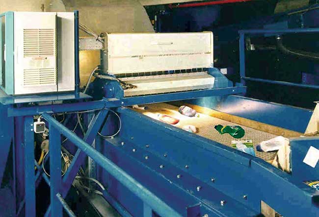
Figure 4. A sorting machine for plastic bottles samples spectra from multiple fiber optic ports across the conveyor belt to sort plastic bottles by type. Courtesy of LLA Instruments GmbH.
High-end LWIR cameras are very expensive because of their cryogenic cooling requirements, but lower cost microbolometer cameras are an alternative. They are, however, limited to frame rates of 30 or 60 Hz and their calibrations tend to drift. This requires a mechanical shutter to create a new nonuniformity correction every few minutes, which reduces long-term reliability and disrupts data acquisition of continuous processes.
SWIR cameras are an alternative to LWIR technology for monitoring industrial hot processes. Manufacturers of InGaAs, like Sensors Unlimited, offer SWIR cameras that:
-
hold their factory uniformity corrections for life
-
have no moving parts
-
provide 640 × 512 pixels with 25-µm pixels with frame rates over 109 fps
-
offer windowing to achieve high frame rates of over 3200 fps for a 64 × 64 region of interest (Figure 5).
High-performance InGaAs cameras see hot spots over 120 °C in low-level ambient lighting, over 150 °C in room lighting, and are regularly used to inspect hollow glass bottle manufacturing lines. The systems verify the dimensions of the product and find defects on both the inside and outside of the bottle, while also monitoring the temperature and its uniformity across the bottle (Figures 6 and 7).

Figure 5. Commercial SWIR imaging cameras come in various camera sizes for 320 × 256 and 640 × 512 pixel image sensor formats (left). On the right is a commercial SWIR digital line-scan camera with a 1024-element linear array that features square 25-μm pixels.
In metal processing, separating the good from the bad is a critical process. The intensity of the light changes as the process proceeds because of differences in emissivity between materials. Though this light intensity change is detectable by a variety of camera technologies, a much better signal-to-noise ratio is achieved in the SWIR waveband because of changes in emissivity as a function of wavelength for different materials. SWIR cameras are also less affected by light scatter caused by smoke and haze than visible cameras while still being able to monitor the process from a distance through the use of inexpensive long focal length lenses.
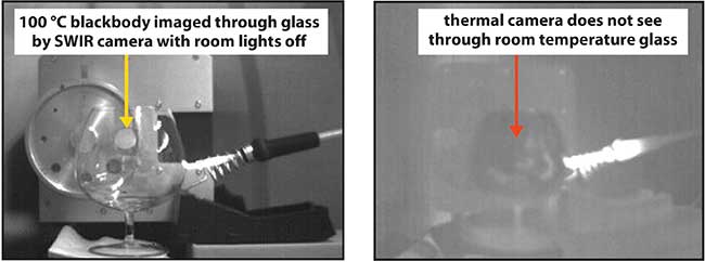
Figure 6. SWIR image (left) and thermal microbolometer image (right) of 100 °C blackbody source imaged through a cognac glass with a soldering iron set at 177 °C. The image was taken in dim room light with similar field of view and image size of 320 × 240 pixels. Note that in the image on the right, the room temperature glass prevents the thermal camera from detecting the light from the blackbody source.
Additional applications, where optical window and lens requirements dictate the use of SWIR InGaAs cameras, are process monitoring of high-temperature chemical recovery processes and inspection of combustion furnaces and components. In many of these cases, filters are employed to block the light emitted by the flame in order to permit the camera to view the walls and the furnace bed in order to determine if maintenance is required. InGaAs cameras have been replacing near-IR vidicon tubes in furnace inspection applications due to their high resolution, low lag, long lifetime, and superior signal-to-noise performance.
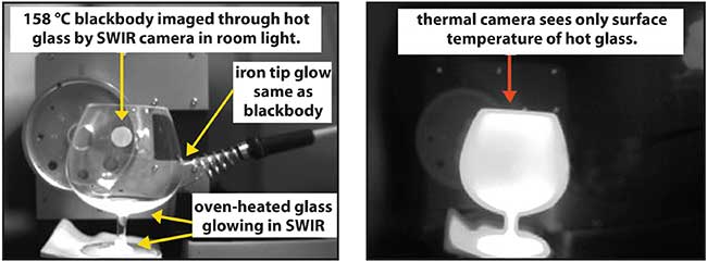
Figure 7. SWIR image (left) and thermal microbolometer image (right) of 158 °C blackbody source imaged through an oven-heated cognac glass with a soldering iron set at 177 °C. The image on the left was taken in full fluorescent room light with SWIR camera integration time reduced by a factor of two from Figure 6. Notice the hot base of the glass in the SWIR image and note that the intensity of the glow from the iron tip is similar to that of the blackbody.
Industrial process monitoring in the SWIR offers process engineers a great tool to enhance current machine vision systems by imaging beyond the visible. Working closely with the system integrator and camera manufacturer, product quality, consistency and yield can be greatly improved, a sure recipe for improving an organization’s bottom line.