Zecotek: Keys to Rapid Success
VANCOUVER, British Columbia, Aug. 8, 2008 – For Zecotek Photonics, the key to its rapid success doesn't lie in cutting-edge technology, an impressive slate of products, a talented team of researchers or strong industry partnerships. The key is having all four.
 Formerly known as Zecotek Medical Systems, the company manufactures crystals, photodetectors, lasers, imaging and 3-D display technologies for medical, biotechnology, industrial, nanotechnology and atomic/molecular science applications. It was founded five years ago by Dr. A.F. Zerrouk in an effort to fund the final phase of research and development of an array of photonics technologies and to guide them through the production and commercialization stages.
In 1989, Zerroul established the first foreign-partnered, private, business-oriented photonics research laboratory in the former Soviet Union, in Novosibirsk, Siberia. He duplicated the same model in three research institutes in Moscow. He has acted as a technology transfer adviser, working closely with the Ministry of Science and Technology during the transition period to the Russian federation. He worked on R&D strategies for the new economy with members of the Russian Academy of Science and coordinated many government projects in joint relations between Russia and countries such as China, Germany, the US, Malaysia and Saudi Arabia.
Zerrouk has been chairman and CEO of various companies in Europe and Asia and has held research and faculty positions at Clarendon Laboratory, the University of Oxford, UK (atomic and laser physics); the Siberian Academy of Sciences (Tokamak and laser fusion research); the Institute of Thermal Processes, Moscow (high-power gas dynamic lasers) and the Institute of General Physics, Moscow, among others.
The Zecotek scientific team has decades of experience in the field of crystal optical materials. Its scientists have introduced many well-known crystals and continue with its comprehensive research program focused on laser media and scintillation materials.
Zecotek operates three divisions in Singapore – Laser Systems, Imaging Systems and 3-D Display Systems – and develops laser systems and components, advanced crystals, solid-state photodetectors, and other imaging and 3-D display technologies for markets including materials processing, bioscience, high-energy, new materials, research, multimedia and security.

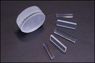
Zecotek’s high-performance scintillation crystal material, LFS, is a key component in the design of whole-body positron emission tomography (PET) scanners and in other industrial applications. (Images courtesy of Zecotek Photonics.)
In December 2004, a year after being established, Zecotek's new subsidiary, Zecotek Crystals Inc., was acquired, with its proprietary high-performance scintillation crystal material – LFS – is a key component in the design of whole-body positron emission tomography (PET) scanners and in other industrial applications.
The mass production and marketing of LFS has been licensed to Northrop Grumman under a long-term contract. To bring production of the new material to a commercial level, the company is setting up a research lab and crystal growth unit in its Singapore facilities. This will be equipped with dedicated Czochralski crystal pulling furnaces as well as with the necessary equipment and machinery to cut and polish the grown material.
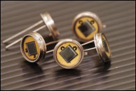
Paul Scherrer Institute in Switzerland is using both Zecotek’s LFS scintillation crystals and MAPD (micropixel avalanche photodiode) photodetectors in its next-generation PET medical imaging program. The Institute for High Energy Physics Research in Russia is using the MAPD photodetectors in a new high-performance hadron calorimeter, to be used in key experiments at the European Centre for High Energy Particle Physics (CERN) in Geneva, Switzerland. The University of Geneva also has selected the photodetectors as an alternative to photomultiplier tubes (PMTs) in the development of new calorimeters for high-energy physics.
Zecotek is leading a collaborative research program with the University of Washington to develop a proprietary PET-MRI detector as the core technology of a new generation of medical imaging systems. The major barrier to a combined PET and MRI scanning device is the strong magnetic fields of MRI, which destroy the photodetection capabilities of current PET scanning devices. Unlike the vacuum-tube-based PMT, Zecotek’s MAPD photodetectors can operate in a highly magnetic environment of the MRI, making the LFS scintillation crystals and MAPD photodetectors critical enabling technologies for a successful fusion of PET and MRI into one scanning device. This new-generation device will offer both higher resolution and faster patient throughput, which, in turn, will improve patient diagnostics and reduce costs to the medical system, Zecotek said.

Zecotek's MAPD (micropixel avalanche photodiode) is being incorporated into next-generation PET medical imaging programs and in key experiments at CERN in Geneva.
Zecotek announced in mid-April that it had successfully completed preproduction testing of the MAPD, which will be initially produced in an 8 × 8 format, with 64 individual MAPDs, each measuring 3 × 3 mm, and scalable to larger dimensions. First-run production has been slated for evaluation by select industry partners. Existing photomultiplier tube markets where Zecotek’s MAPDs offer both cost and performance advantages include: medical inspection devices used in blood analysis and DNA sequencing, gamma ray detectors for homeland security, environmental monitoring, industrial control systems, robotics, biomedical testing, navigation and guidance systems, laser radars and high-energy physics, the company said.
“Our 64-chip MAPD array has been specifically designed for use with our LFS scintillation crystals in medical scanning applications," Zerrouk said. “Their unique performance and design attributes provide a significant opportunity for new detection configurations, which allows for higher resolution, more conclusive medical interpretation of data and images, and new applications in positron emission tomography. In addition, the array has a wide range of applications in high-energy physics, security and other imaging industries. We are delighted with the strong interest and support we are receiving from key industry players."
Zecotek Laser Systems Pte Ltd. manufactures lasers, laser materials and components: high-performance vanadate laser cavity crystals, fiber lasers for medical, instrumentation and materials processing applications (green- and blue-emitting and Raman), ultrawide tunable lasers for scientific applications, diode-pumped solid-state lasers for biomedical applications, and thin-film lasers.
It has labs in Canada, the US, Singapore, Malaysia and Russia, with its main in-house production facilities in Singapore and Novosibirsk. The company has outsourced high-volume product manufacturing through strategic alliances with Northrop Grumman in the US, Fujikura Ltd. in Japan (for fiber and solid-state laser systems), the Malaysian Institute of Microelectronics (for solid-state MAPD photodetectors), and Anteryon BV in the Netherlands for a key component of the 3-D display screen.
Senior management determined in early 2006 that it would benefit the company and its shareholders if Zecotek integrated its technologies into higher value-added components and manufactured some of its own products, so it chose manufacturing and commercialization facilities in Singapore and Malaysia.

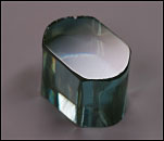
Zecotek produces these high-performance rare-earth fine oxide (RFO) vanadate laser crystals, eyed as a superior replacement to YAG crystal –used in about 60 percent of all laser crystal applications – and as a light source for optical coherence tomography.
In December 2007, Zecotek gained approximately $5 million in equity unit financing, which will be used for working capital purposes and for ongoing projects currently under way at its facilities in Singapore, Malaysia and Vancouver: finalizing the commercial production of the solid-state MAPD photodetector, addressing growing requests for its fiber and solid-state lasers, initiating commercial-scale production of high-performance RFO vanadate laser crystals (a key component in solid-state lasers) and establishing a manufacturing and distribution partnership for its 3-D display system.
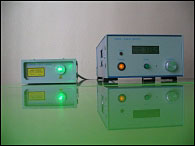
The company's 540- and 550-nm series green fiber lasers offer applications in genomics, flow cytometry and confocal microscopy.
“Much of the heavy lifting in research and development is completed, and we have now turned our attention to commercializing our technologies,” Zerrouk said. “We have attracted key strategic partners with Fujikura, Northrop Grumman and the Malaysian Institute for Micro-electronics Systems, and we are gearing up for commercial production. Our photonics technologies have caught the attention of highly respected scientific organizations, and sales are increasing. We remain focused on executing our business plan, increasing shareholder value, and [we] thank shareholders for their continued support.”
Some new technologies the company is working on include: a real-time autostereoscopic 3-D display; various solid-state and fiber laser technologies, including a solid-state laser for bioinstrumentation, and a thin-film waveguide microlaser technology, the latter being currently in development jointly with the University of British Columbia (UBC); enabling technologies for combined PET-MRI machines, in development with the University of Washington; a new scintillation material for medical imaging to eventually serve as a successor material to the LFS; a solid-state analog to the existing photomultiplier tube; the RFO crystal, eyed as a superior replacement to the present YAG crystal; and a light source for optical coherence tomography, in development in conjunction with UBC.
Zecotek has demonstrated a fully operational 32-in. commercial prototype of its proprietary Real-Time 3D2D Display System, the first 3-D display offering multiple viewers true volumetric visualization while exhibiting depth and parallax over a wide viewing angle. Demonstrations have been held at the company’s Vancouver laboratories to a select group of representatives of potential industry partners. Anteryon BV of the Netherlands is producing the proprietary 3-D lenticular display in the 32-in. screen format, considered the optimum size to demonstrate its potential power and user impact. The design provides for multiuser, multiview, freedom of movement, high resolution in both 3-D and 2-D modes, superior image dynamic range in 2-D mode, 2-D and 3-D simultaneous displays, common brightness and compatibility with existing applications. It also is designed to be cost-competitive.
“We continue to successfully execute our business strategy of bringing photonics technologies to market through strong industry partnerships,” Zerrouk said. “In February 2008, we signed a manufacturing, commercialization and joint development agreement with Fujikura Ltd. of Japan. By combining Fujikura’s outstanding manufacturing and product engineering capabilities with Zecotek’s strength in innovation, patents and product portfolio, we have created a new world-class laser enterprise with outstanding market potential.
“Furthermore, we have strengthened our internal marketing programs and have participated in a number of events such as the Photonics West trade show and the IEEE Nuclear Science Symposium, which have noticeably accelerated both inquiries and orders for all of our product lines. Our full range of laser products, high-performance crystals and solid-state photodetectors are meeting and exceeding quality and production parameters with a growing list of key US and European customers.”
With the announcement of a manufacturing and distribution agreement with Fujikura, Zecotek said it is positioned to become a leading supplier in the global laser systems and components industry. The relationship will immediately focus on producing Zecotek’s green fiber laser and Zecotek/Fujikura joint high-power visible fiber laser for laser machining. The companies will pool resources to manufacture new lines of visible wavelength lasers aimed at significant markets in bioinstrumentation and the processing of a wide range of industrial, consumer-based and research materials.
The company also signed Toyo Ram as its Israel distributor for its green fiber and ultrawide tunable lasers, MAPD photodetectors combined with the LFS scintillation material, and RFO vanadate laser crystals.

Zecotek's green fiber laser series provides wavelengths from 515 to 560 nm, suitable for biosinstrumentation, medical, material processing and research applications.
In recent months, Zecotek has strengthened its sales and marketing efforts and participated in key trade shows, both of which have significantly increased sales inquiries and orders. It exhibited in May at the Conference on Lasers and Electro-Optics (CLEO) in San Jose, Calif., demonstrating its 540- and 550-nm green fiber lasers and other advanced products and has sold products to the Department of Physics, University of Illinois, Urbana-Champaign; Institute for Quantum Computing, University of Waterloo, Canada; Gwangju Institute of Science and Technology in Korea; and the National Institute of Health in the US.
The National Cancer Institute (a division of the US National Institutes of Health) recently conducted tests on Zecotek’s green fiber laser (GFL-550) in flow cytometry. William Telford, head of the Flow Cytometry Core Laboratory at the institute, presented a paper about the GFL-550’s performance and 550-nm wavelength at the 24th International Congress of the International Society for Analytical Cytometry, held last year in Budapest, Hungary.
Zecotek’s GFL series also provides wavelengths in the 515- to 560-nm range, suitable for bioinstrumentation, medical, materials processing and research applications. The series will be manufactured by Fujikura under a joint agreement.
Zecotek said its 336-nm DPSS laser offers both better performance and longer lifetime than existing lasers used in mass spectrometry based on the Maldi-Tof (matrix-assisted laser desorption/ionization-time of flight) technique, which is rapidly becoming the most widely used tool in biomolecular analysis and an important tool in quality control because of its high throughput capabilities and ease of automation.
"We have an opportunity to meet the growing demand of Maldi-Tof laser systems," Zerrouk said. "Our 336-nm DPSS laser has been specifically designed to replace the cumbersome and shorter life-span nitrogen gas lasers used in legacy systems. Zecotek is in the position to offer a major component to OEMs for their new-generation Maldi-Tof systems."
The solid-state 336-nm DPSS laser program is based in the company's Singapore labs and patent applications are being prepared. The first laser was available for customer sampling last August. The first small-volume production were done at Zecotek's facilities and small quantity orders of the laser fulfilled beginning in October. Product ramp-up will be transferred to Fujikura for mass production.
For more information, visit: www.zecotek.com
/Buyers_Guide/Zecotek_Photonics_Inc/c17047