
ZEISS Opens China R&D, Manufacturing Site: Week in Brief: 7/12/24
SUZHOU, China, July 12, 2024 — ZEISS, a developer of optics and optoelectronics, has opened a new R&D and manufacturing site at the Suzhou Industrial Park in Suzhou, China. The 13,000 sq m site will be used to produce industrial quality solutions, research microscopes, surgical microscopes, and ophthalmic equipment. This opening marks the group’s first land purchase for its self-built project in China.
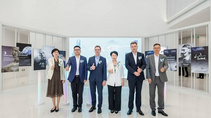
Representatives of the Suzhou Industrial Park and ZEISS at the site’s opening. Courtesy of ZEISS.
KINGSTON, Ontario — Semiconductor facilitator and accelerator CMC Microsystems and Innovation, Science, and Economic Development Canada (ISED) have launched FABrIC, an initiative meant to provide financial and technical resources, mentorship, and training for semiconductor businesses, engineers, and scientists in Canada. Powered by a 120 million CAD ($88 million) investment from ISED’s Strategic Innovation Fund, FABrIC will enable the training of 25,000 students, and 1,000 professors over 5 years, and provide Canadian universities and colleges with technical resources for students and researchers to design and manufacture advanced semiconductor devices during their studies.
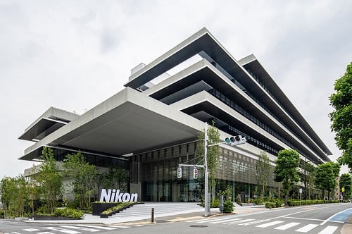
Nikon’s current global headquarters site in Shinagawa City. Courtesy of Nikon.
TOKYO — Nikon Corporation, a developer of optoelectronics-based technologies, plans to relaunch subsidiary Morf3D as Nikon AM Synergy Inc. The rebranding includes new leadership and a shift from the former general-purpose contract manufacturing service bureau business, leading to the closure of the El Segundo, California location and the divestment of non-essential equipment. The subsidiary will instead operate from Nikon's advanced manufacturing business unit facility in Long Beach, California. This comes as Nikon plans a relocation of its global corporate headquarters within Tokyo, from the Shinagawa City ward to the Minato City ward.
TUCSON, Ariz. — Ultrashort pulse laser technologies company Applied Energetics, Inc. has exercised its option to lease more than 5,000 sq ft of additional space at the University of Arizona Tech Park. The additional space will support the company's investment in a new battle lab and laser manufacturing capacity to ensure it has the infrastructure in place to fulfill both current and possible future priority U.S. military programs. The total 26,000 sq ft space will include a high bay, light industrial facility that is expected to enable technology maturation and be the venue for customer and partner demonstrations under realistic and controlled conditions. The facility will also provide the capability to manufacture, integrate, and test advanced lasers.
WALTHAM, Mass. — Thermo Fisher Scientific Inc., a medical technologies company, has completed its acquisition of Olink Holding AB, a provider of proteomics solutions. The transaction values Olink at approximately $3.1 billion with a net of $96 million of acquired cash. Olink will become part of Thermo Fisher's Life Sciences Solutions segment.
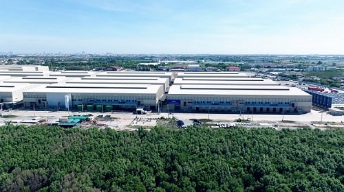
HSG’s new Bangkok manufacturing facility. Courtesy of HSG Laser.
CHICAGO — Metal shaping equipment and solutions company HSG Laser has opened its first manufacturing facility in Bangkok as part of its global expansion strategy to support its growing international customer base. The 10,000 sq m facility includes laser cutting production lines with flat cutting, tube cutting, sheet cutting, 3D five-axis cutting, and automation solutions. The company expects the new facility to produce 2000 units annually, contributing to an annual global production capacity of more than 10,000 units. The company has locations in China, North America, Europe, and Japan.
Kodifly’s Islamabad office within the National Science and Technology Park. Courtesy of Kodifly.
HONG KONG — Kodifly, a provider of spatial intelligence solutions for infrastructure management, has opened a new office in Islamabad in an effort to strengthen its presence in the South Asian and Middle Eastern markets. The facility will serve as an R&D center, as well as house a team of engineers, data scientists, and client success professionals. This comes after Kodifly’s $750,000 funding round led by Laidlaw Scholars Ventures to support the productization of the company’s solutions, which use machine learning to create digital twins of environments with lidar and real-time video analytics within urban environments.
COLORADO SPRINGS, Colo. — Geospatial data and solutions company The Sanborn Map Company Inc. has acquired the assets of Geiger mode lidar specialist VeriDaaS for an undisclosed amount. Sanborn will integrate VeriDaaS’ assets and solutions, including asset management, vegetation management, solar sighting, flood risk and resilience, wildfire management, and urban change analysis among other applications, into its Mapping Division and linear mode lidar technology.
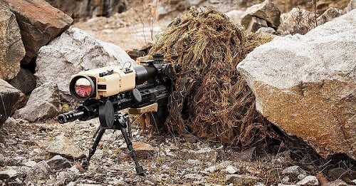
The ThermoSight HISS-XLR weapon sight shown being used by a soldier. Courtesy of Teledyne FLIR Defense.
BOSTON — Teledyne FLIR Defense has received a $15 million contract through the U.S. Army Contracting Command-Aberdeen Proving Ground to deliver more than 150 of its ThermoSight HISS-XLR weapon sights to a NATO partner country. The contract also includes parts, training, and other in-country support. The ThermoSight HISS-XLR clip-on thermal weapon sight enables detection of targets at more than 2000 m. Work will be performed at FLIR Defense’s manufacturing and service facility in Billerica, Massachusetts, with deliveries beginning in the spring and continuing through 2024.
MADRID — High-speed connectivity over fiber optics supplier KDPOF has established a packaging plant for optoelectronic devices close to its headquarters in Tres Cantos, Spain along with a prototype laboratory for testing its own products. Bolstered by a €26.8 million (~$29 million) Important Project of Common European Interest (IPCEI) investment from the European Commission, the encapsulation and testing factory for large volumes will go into operation in 2025 and is set to produce its transceiver IC for high-speed automotive optical communications. Along with the opening of its new facilities, KDPOF will be rebranding as KD.
/Buyers_Guide/Carl_Zeiss_Spectroscopy_GmbH/c16323
/Buyers_Guide/CMC_Microsystems/c31346
/Buyers_Guide/Nikon_Corp_Digital_Solutions_Business_Unit/c10300
/Buyers_Guide/Applied_Energetics_Inc/c18272
/Buyers_Guide/Thermo_Fisher_Scientific_Inc/c20775
/Buyers_Guide/Teledyne_FLIR/c5030
/Buyers_Guide/KD/c31233