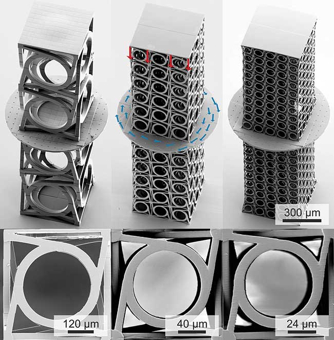
3D nanoprinting may soon merge into mainstream manufacturing thanks to increased throughput and refined lasers, optics, and materials.
 Copies of buildings and the Statue of Liberty that are only microns tall — these are examples of what’s been done with three-dimensional nanolithography, known as 3D nanoprinting. Also possible today is the manufacturing of optical, photonic, microfluidic, and other components on the nanoscale. Compared to mask lithography and large-scale manufacturing methods, 3D nanoprinted components offer solutions that can be less expensive, better performing, quicker to create, and more compact.
For instance, in February 2018 researchers at New York Genome Center and New York University reported on a 3D-printed, low-cost, microfluidic system for single-cell analysis, demonstrating the usefulness of the approach in a clinical environment. Thanks to custom printing of the central device, the total cost of the system was a fraction of a comparable traditional solution, and it had a smaller footprint.
Microscopic 3D manufacturing depends upon lasers, positioning systems, and photosensitive materials with the right properties. Hence, advances in these areas are required if 3D nanoprinting cannot currently satisfy requirements, such as hitting cost targets.
But, in some applications, 3D nanolithography already offers the necessary performance in terms of quality and cost. A case in point is diffractive-refractive optics, which can increasingly be found in the time-of-flight and lidar technology in products such as self-driving cars. For such optics, 3D nanoprinting can do what conventional manufacturing cannot.
“Conventional lenses with a size down to a micron diameter can be produced by diamond turning, but other DOEs (diffractive-refractive optical elements) have a structure size in the nanometer area,” said Peter Pagnin, the European business development manager for Singapore-based Moveon Technologies Pte. Ltd., in explaining why diamond turning is not suited for the task.
In the past, manufacturers relied on a mask-based lithographic process to make these fine-feature optics, which meant masks had to be designed and manufactured first, and then components were made using those masks. This mask-and-component process had to be repeated with each development turn. During prototyping, several cycles were often needed.
That’s why Moveon turned to a two-photon, 3D nanoprinting process for a rapid and inexpensive prototype turnaround of microlens arrays, mirrors, and other DOEs. In it, an NIR laser fires femtosecond pulses, which are focused within a UV photocurable resin that sits on a substrate. The intense light of the pulse at the focal point exceeds a threshold, leading to two-photon absorption and polymerization of the resin. This spot can be moved around as desired by shifting the stage, the beam, or both.
Member Exclusive: To read the complete article, please Login or Register