Robert Ferguson, National Physical Laboratory, UK
Measuring the attenuation and isolation of polymer waveguides in optical printed circuit boards will help manufacturers develop and produce better boards for optical communications.
The demands of high-speed data transfer in modern computing and data storage systems have driven the development of optical printed circuit boards (OPCBs) to the point where viable devices are now beginning to appear. The bandwidth capacity, size and lower energy demands of these boards ensure continuing interest among international communications companies.
Test and measurement are vital steps in the fabrication of boards or backplanes, but the actual waveguides themselves also must be characterized. Knowledge of the guides’ attenuation and isolation is critical to their operation and to the development and refinement of the boards.

Figure 1. Images showing various illuminated waveguides for different types of optical printed circuit boards. Images courtesy of National Physical Laboratory.
Figure 1 shows the edges of different boards with illuminated polymer waveguide end faces. Variations in the launch numerical aperture (NA), defined here as the sine of the half angle of the launch cone of light entering the fiber, can lead to very large differences in the measured total attenuation values (Figure 2). The attenuation of multimode polymer waveguides is more likely to be mode-dependent than that of single-mode fiber because of the larger propagation angles and core dimensions in the former.
A variable launch system from the National Physical Laboratory in Teddington, UK, measures the attenuation and isolation of the polymer waveguides found in these boards. The flexible system can accommodate a variety of board and waveguide sizes.
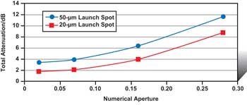
Figure 2. A typical plot of total attenuation against different launch numerical apertures and spot sizes for a typical polymer waveguide.
The amount of crosstalk – light leaking into adjacent guides – is as important a criterion as is the attenuation of a particular waveguide. Manufacturers of these boards also need to know the end-face quality of the guides. Assessments can be made for both surface roughness and geometrical form, and the corresponding coupling losses into and out of the guide can be determined.
Understanding the launch condition
The dimensions of these guides are typically 75 x 30 µm and consist of the polymer guide material overlaid with a material of a suitably lower refractive index. Although apparently simple in concept, real difficulties must be overcome to maintain integrity throughout the guide’s length. The inclusion of various radii and crossover structures in more complex boards adds to the need for good metrology. Because the guide can support many modes, attenuation values are tied to the conditions of launch, which must be specified. It is important to note that the measured total attenuation of the waveguide includes the propagation losses (intrinsic and extrinsic, including joint and bend losses as well as the effects of side-wall roughness) and the coupling losses associated with the end faces (Fresnel reflection and surface scattering losses):
Total attenuation = Propagation losses + Coupling losses
The new system can reproduce specific launch conditions. The launch spot size can be selected using a laser-punched series of pinholes, and the NA can be defined with a variable aperture to fully explore the capability of these multimode waveguides. The system can overfill and underfill the waveguide, thereby exciting different propagating modes within the guide. Figure 3 shows part of this system with a board mounted between the launch and receive objectives. Operating using an 850-nm vertical-cavity surface-emitting laser source, the spot sizes range from 5 to 100 µm, and the current NA range is 0.02 to 0.28.
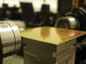
Figure 3. An optical printed circuit board mounted and aligned with respect to the launch and receive objectives.
Ideally, the launch condition can be preselected to match the launch condition of the board in its operating state. One-to-one system imaging ensures the correlation of the pinhole diameter to the spot that falls on the front face of the guide under test. A CCD allows viewing and careful positioning of the spot on the front face. Figure 4 shows a typical image from the launch CCD with a spot positioned on the waveguide. With this particular board, light is clearly leaked into the adjacent guides.
The measuring process
Once the correct launch condition is selected, the transmitted output power from the guide is measured using a characterized CCD. A reference signal using the same launch condition is measured with the guide removed. This allows the ratio of the transmitted power to the reference power to be determined. The total attenuation, A, in decibels, of an optical waveguide within an OPCB is defined in Equation 1, where P0 represents the power entering the input surface of the waveguide and P1 the power exiting the waveguide. Because the measured attenuation includes all the loss components of the waveguide, it can be termed the insertion loss. Throughout, any fluctuations in the source output power also are monitored using a reference detector and are eliminated from the final values.

Figure 4. A CCD image showing the 50-µm launch spot centrally located on the input face of a 70 x 50-µm waveguide.
The use of a CCD allows imaging of the output signal and setting of a software-generated virtual pinhole to capture all the light exiting the waveguide, and it corresponds to the expected photodiode that is intended for the OPCB, typically 70 µm in diameter. The diameter of this virtual pinhole can vary between 50 and 200 µm.
Crosstalk also can be carried out on more complex boards where radii and crossover structures are incorporated within the board design. With a waveguide spacing of ~200 to 250 µm, the CCD can accommodate the output signals from several guides. This allows isolation measurements of the first- and second-order guides to be carried out. The isolation is derived by the ratio of the total illuminated waveguide output power divided by the total neighboring waveguide output power.
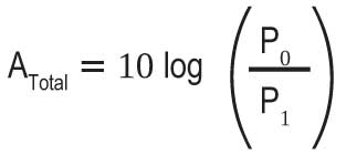
Figure 5 shows an example of the output isolation levels between adjacent guides. In this case, the level between first- and second-order guides is ~13 dB. The corresponding CCD image shows the virtual pinhole diameter that defines the area in which the total power of a particular guide is measured.
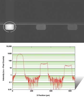
Figure 5. Isolation investigation across adjacent waveguides showing measured output crosstalk in first- and second-order guides. The corresponding CCD image shows the virtual pinhole diameter that defines the area in which the total power of a particular guide is measured.
Attenuation measurement uncertainties include contributions associated with the launch and the waveguide condition, the power measurements as well as the measurement repeatability and reproducibility. For low attenuation waveguides of <2 dB, an uncertainty of ±0.25 dB has been assigned at the 95 percent confidence level. This can increase to ~1 dB for waveguides with a loss of 25 dB.
Coping with increasing complexity
Larger and more complex OPCBs with greater numbers of guides are envisaged for the near future. The new measurement system allows for a wide range of board dimensions and configurations accommodating boards from approximately 50 cm down to ~1 cm. It also can measure waveguide outputs up to 90° to the input, increasing the flexibility.
Besides planar waveguides, other guides involving radii and crossovers have been measured using a 50-µm launch spot and a 70-µm virtual pinhole on the receive CCD, and with an NA of 0.16. Preliminary results showed that the inclusion of relatively shallow radii in a waveguide of 15 mm can produce a relative increase in loss of between ~3.1 and 4.5 dB, depending upon the launch NA and an increase in the attenuation coefficient of ~0.32 dB/cm, indicating a notable increase in propagation loss resulting from the deviation of the waveguide path.
The inclusion of further similar bends in the length of the guide increases the total attenuation resulting from the increase in overall guide length but shows little difference in the measured attenuation coefficient. More work is intended to investigate a range of bend radii.
The same launch conditions were applied to measure boards containing a range of crossing structures to simulate actual waveguide crossing points (Figure 6). Each board contained planar waveguides as well as guides with structures possessing various crossing angles, grouped in batches of 10. The loss per crossing structure was determined by comparison with the respective planar guides on each board. Greater attenuation was found for low crossing angles, with the loss per crossing structure for a 10° angle as high as ~0.4 dB, reducing to about 0.2 dB for a 30° crossing angle. Crossing angles greater than 60° reduced the loss per crossing structure to ~0.13 dB for 10 crossings to a minimum of about 0.05 dB over 100 crossings as a modal power distribution steady state is reached.
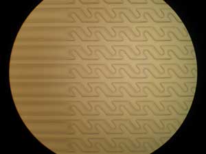
Figure 6. A series of adjacent waveguides showing repeated 60° crossing structures in a prototype optical printed circuit board.
This system is intended for systematic study of the attenuation and isolation of these and other optical waveguides as a function of the optical launch. Further measurements are planned on prototype boards produced using a variety of processes. As these boards become established as high-speed computer backplanes, the system can provide the necessary means to characterize them and enable the manufacturers to improve their technology.
Further development of the system will increase its operating dynamic range, and an investigation into the coupling loss component associated with the quality of the waveguide end faces is expected.
Meet the author
Robert Ferguson is a higher research scientist at National Physical Laboratory in Teddington, UK; email: [email protected].