Derek Mendes, Imtec Acculine LLC
With far higher etch rates and per-unit cost savings, high-temperature wet etching of sapphire wafers is giving dry etching a run for its money.
LED manufacturers today can choose between two very different manufacturing processes. Dry etching creates efficient, bright LEDs – but it does so slowly and with limited throughput. And wet etching is very scalable and fast, but the LEDs it produces are less effective and less efficient.
Wet etching requires polishing touch-up work on the wafers to increase light-extraction efficiencies, but it still results in a considerable cost savings over dry etching. It also scales much more efficiently, multiplying the savings dramatically as throughput and wafer size increase.

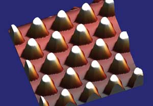
High-temperature wet etching of sapphire wafers results in the creation of truncated cone shapes: conical structures with flat tops. Images courtesy of Imtec.
“Say you look at a flat substrate, and then you make a patterned substrate – the cost of making a patterned substrate increases the cost by 20 percent or maybe 25 percent,” said Rajiv K. Singh, vice president, co-founder and chief technology officer of Sinmat Inc. “The wet etch would decrease that added cost by half.”
LED manufacturers must cut costs wherever they can, while still maintaining or improving quality. And although larger-diameter sapphire wafers hold promise for making the manufacturing process significantly more efficient, they also present challenges to fabricators.
Using a 4-in.-diameter wafer instead of a standard 2-in. one quadruples the wafer’s available surface area. Moving from a 4-in. wafer to a 6-in. one doubles the surface area, and every subsequent jump in size further increases it.
But if existing manufacturing equipment cannot cheaply or easily scale up to accommodate the larger form factors, the theoretical gains in efficiency with larger wafers are canceled out.
Patterned sapphire substrates (PSS) play two roles in the LED industry. On the wafer-supplier side, they mean dollar signs: PSS wafers represent higher gross margins than traditionally polished sapphire ones. And on the product development side, LEDs based on PSS wafers are more efficient and more effective as light sources.

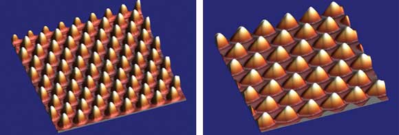
Formerly flat, truncated shapes polished and rounded (left) now more closely resemble dry-etched PSS patterns (right).
“The PSS reduces the dislocation density in the GaN layer and enhances the light extraction efficiency (LEE) from the LED chip by scattering the light confined in GaN layer attributed to the critical angle between GaN (n = 2.4) and sapphire substrate (n = 1.7) (or air (n = 1.0),” wrote Kazuyuki Tadatomo and Narihito Okada of Yamaguchi University in Japan in a 2011 paper.1
Dry etching
The most common method for producing PSS wafers is dry etching, whose techniques and technology are commonplace, including the inductively coupled plasma variant lithography. This process exposes a pattern onto the photoresist of the sapphire substrate and anisotropically etches it into the crystalline structure via exposure to fluoride-based plasma gas and microwave energy. The resulting pattern – highly uniform, densely packed and dome-shaped – encourages lateral film growth, which, in turn, means fewer defects and increased light refraction.
Although LEDs based on dry-etched PSS wafers are highly efficient light sources, the process is slow. A standard 2-in. wafer can take between 30 and 60 min to etch, depending upon the depth of the pattern being etched and the type of film used. Average rates are practically impossible to define because of all the possible process variables, but dry-etching rates generally range between 50 and 200 nm/min, or 20 min/µm.
The dry-etch process also cannot be effectively scaled. The throughput of a dry etcher decreases as wafer size increases because, as the size goes up, fewer wafers will fit inside the vacuum chamber. This means that more expensive plasma-etching tools are required for bigger wafers if throughput is to remain comparable. And more tools mean more operational costs: facilities, utilities, maintenance and consumables.
Wet etching
In contrast, the high-temperature wet-etching process is comparatively much cheaper than dry etching – and faster, too.
During high-temperature wet etching, wafers coated with gallium nitride or indium gallium nitride (InGaN) are placed in a tank with a mixture of etching and buffering agents: sulfuric and phosphoric acids, typically in a 1:1 or 3:1 ratio. Before submersion, a plasma-enhanced chemical vapor process spins a silicon dioxide mask onto the sapphire substrate, and lithography exposes the required pattern. The mixture is brought to temperatures ranging between 260 and 300 °C – much higher than those used in traditional semiconductor fabricating, which typically run between 150 and 180 °C.
Etching rates do not increase along a linear scale as temperatures rise. Instead, they increase exponentially, so that a 300 °C temperature may make etching twice as fast as at 260 °C. On the other hand, “the etching rate increased linearly when the H2SO volume ratio increased from 0 to 75 percent,” as reported by D.S. Wuu of National Chung Hsing University in Taiwan and colleagues.2
High-temperature wet-etching rates can be measured in microns per minute; a rate of more than 1 µm/min is achievable under the correct conditions, according to Sinmat’s Singh, who added that it is reasonable to expect full etching of a standard 2-in. wafer in five minutes. And with regard to cost, a process tank for a batch of 6-in. wafers is only slightly more expensive than a tank designed for a batch of 2-in. wafers – and it can hold the same number of wafers.
Of course, using extremely hot chemicals can be challenging for manufacturers: Safety is paramount with chemicals hot and powerful enough to rapidly etch sapphire surfaces. To maintain safety, any system must feature a suitable chemical tank, designed not to react with any of the chemicals. Preferably it will be constructed of a sturdy substance such as high-purity virgin annealed quartz. No plastics should come into contact with the chemical mixture, and built-in temperature sensors should feed precise readings back to the systems management equipment. As added safety features, some tanks include a cooldown module to house the hot chemistry while it cools and overflow tanks that can hold 120 percent of the main tank’s volume in case of an accident.
Wet-etching research
A sapphire-wafer producer in Japan recently concluded testing of the Imtec Acculine XE-Series bath. The experiment compared uniformity, etch-rate and structure-formation data with previous in-house test results. The company especially noted the tight temperature control throughout the bath, which aided etch uniformity. Also cited was the ability of the bath temperature to recover quickly once a new batch of five 2-in. wafers was loaded into the 280 °C solution. Testing will continue on 6- and 8-in. sapphire wafers, and similar results are expected.

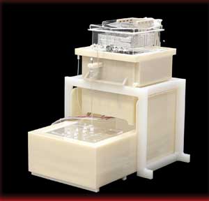
The Imtec Acculine XE-Series tanks are constructed of virgin annealed quartz and contain no plastics that come in contact during use of high-temperature chemicals. The XE-Series also includes a cooldown module and an overflow tank in case of an accident.
The PSS created using the high-temperature wet-etching process is a significant improvement over a nonpatterned wafer in terms of light extraction and efficiency. The process results in the creation of truncated cone shapes – conical structures with flat tops.
Unfortunately, the flattop surface of the cone poses two significant challenges to those used to working with the dry-etching process. The flattop acts to discourage the lateral growth of film and encourage vertical film growth, resulting in more defects. Also, the shape of the structures inhibits efficient light refraction.
Because this is still a relatively new process, research is being conducted into improving the quality of wet-etched sapphire wafers. Sinmat is one company undertaking such research, and it has developed a method to polish the flat structures, producing rounder, more efficient domes that more closely resemble the shape of those produced by the dry-etching process.
Others are investigating the creation of patterns other than cone shapes. At National Chung Hsing University in Taiwan, Jing-Jie Dai and colleagues created “truncated-triangle-striped patterned-sapphire substrate and a rhombus-like air-void structure at the GaN/sapphire interface to increase the light extraction efficiency. The truncated-triangle-striped patterned-sapphire substrate was fabricated through a wet-etching process in hot sulfuric and phosphoric acid solutions. A rhombus-like air-void structure at the GaN/sapphire interface was formed though a wet-etching process along a V-shaped air-void structure on the patterned sapphire substrate.”3
After testing, the researchers concluded that “the [rhombus-like air-void structure LED] has a 65 percent light-output power enhancement, a smaller divergent angle, and a periodic higher light intensity profile compared to a [flat sapphire substrate standard LED] that provides a high external quantum efficiency in nitride-based LED applications.”3
Meet the author
Derek Mendes is the sales/marketing administrator at Imtec Acculine LLC in Fremont, Calif.; email: [email protected].
References
1. T. Kazuyuki and N. Okada (2011). Development of patterned sapphire substrate and the application to the growth of non-polar and semi-polar GaN for light-emitting diodes. Proc. SPIE, 7954, 795416; http://dx.doi.org/ 10.1117/12.874179.
2. D.S. Wuu et al (June 2006). Fabrication of pyramidal patterned sapphire substrates for high-efficiency InGaN-based light emitting diodes. Journ Electrochem Soc, Vol. 153, No. 8, pp. G765-G770.
3. J.-J. Dai et al (2010. Enhanced the light extraction efficiency of an InGaN light emitting diodes with an embedded rhombus-like air-void structure. Appl Phys Expr, Vol. 3, Issue 7, pp. 071002-071002-3.
The Market for LEDs
The high-brightness (HB) LED market experienced a 93 percent growth rate between 2009 and 2010, according to a market research report from Strategies Unlimited. In 2009, the global market for packaged HB LEDs was $5.6 billion; in 2010, it grew to $10.8 billion. The report predicts that the global market will be worth $18.9 billion by 2015, representing a compound annual growth rate of 11.8 percent.
The US Department of Energy is expected to release a report stating that, to compete effectively with the fluorescent lighting market, solid-state lighting manufacturers must cut the cost per lumen (currently at $18/klm) by eight times to $2.20/klm by 2015.