Dr. Jason Smith, University of Oxford
Quantum information technologies are set to revolutionize communication security and computing capabilities over the coming decades, and governments and companies are beginning to invest heavily in development and, in some cases, installation of working systems.1 In the case of quantum key distribution (QKD) for secure communications, the technology is sufficiently advanced that industry standards have been set,2 and a handful of commercial systems are now available.
A basic component of the quantum toolbox is the triggered single-photon source, in which a single photon is produced, on demand, in response to a clock signal or user-generated trigger. This photon can carry quantum information via its polarization, for one example, over long distances as part of a quantum communications system. In QKD, a cryptographic key is generated securely at two remote locations by the exchange of information-carrying photons. It is important here that single photons are used to avoid the possibility of the key being eavesdropped without detection (i.e., a “beamsplitter attack”). In linear-optics-based quantum computing, single photons are used to carry out operations via a series of quantum logic gates. For two-qubit gates to work, these photons must be formally indistinguishable – identical in every respect – to make use of the properties of quantum interference.
Although conceptually simple, the challenges of building a triggered single-photon source for use outside a laboratory environment are considerable, and to date such sources have yet to make an impact on the emerging industry. As a result, in QKD, although the triggered single-photon source is still preferred a priori, alternative methods like entangled and heralded photon sources, weak coherent sources, and continuously variable approaches are more industry-ready and thus dominate the current systems in use. High-specification triggered single-photon sources using semiconductor quantum dots have been realized at low temperatures, but the need to house these devices in cryostats means they are bulky and expensive to produce.
The European Commission-funded Wavelength-tunable Advanced Single Photon Sources (WASPS)
program seeks to change this equation by developing a new generation of triggered single-photon sources based on diamond defects coupled to novel optical resonators. The devices in development promise a range of high specifications including ambient-temperature operation, making them ideal for commercial and industrial settings. The three-year program (running from November 2013 to October 2016) involves a consortium of six European research groups. Their goal is to produce single-photon sources that can facilitate technological advances in both quantum communications and quantum computing, with specific focus on breaching barriers that have prevented previous triggered sources from achieving an industrial impact.
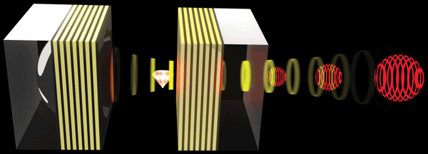
At the heart of each device is a single atomic defect in the diamond crystal, which is situated in an optical microresonator (Figure 1). The defect is energetically excited using a laser pulse and then relaxes back to ground state, emitting a single photon into the microresonator as it does so. In contrast with many other triggered single-photon-emitting materials, the defect within the diamond crystal allows this emission process to work
effectively at ambient temperatures, an important advantage when it comes to building low-cost and user-friendly devices.

Figure 1. A view inside a WASPS single-photon source: A diamond nanocrystal containing a single fluorescent point defect is situated in a miniature optical resonator so that it emits single photons efficiently into a well-defined mode. The photons then escape through the planar mirror, which acts as an output coupler. The entire structure ranges from 5 to 50 μm in size. Photo courtesy of Dr. David Coles.
The microresonator provides a strong optical mode, which is what causes photon emission into it. A high degree of control over this optical mode is a central principle in the design of WASPS devices, not only to provide excellent quality output-beam characteristics but also to boost the efficiency of the device (i.e., the probability that a single trigger event will result in a single photon) and to increase the attainable clock speed. An example of the specifications targeted in the project is a room-temperature, single-photon source with a device efficiency of 80 percent and a clock speed of 1 GHz. The operating wavelengths of the sources typically range from 600 to 800 nm, well-suited for free-space optical systems and short-range fiber or waveguide-based technologies. So far, no known diamond defect emits single photons in the long-range fiber telecommunications bands ¬–
usually ranging from 1300 to 1600 nm – although the core WASPS technology would be readily adaptable if a suitable candidate were identified.
This high degree of mode control produces excellent spatial and spectral properties of the single photons produced. The first devices are being engineered to produce pure TEM00 mode outputs, both free-space and fiber coupled, for efficient integration with a wide range of optical systems. Spectral linewidths are narrow, from 0.001 to 1 nm, without substantially compromising the efficiency or clock speed. Narrow spectral linewidths are beneficial in fiber-based communications because they minimize the deleterious effects of temporal dispersion. Additionally, they are useful in free-space QKD systems because they allow tight spectral filtering to suppress unwanted background noise from sunlight and other stray light sources.
A further advantage of the design used in WASPS is that the photon wavelength can be tuned by the user. Such capability opens the prospect of wavelength multiplexing in quantum communications channels – that is, sending multiple, independent single-photon streams in parallel (by virtue of different wavelengths) through a single waveguide system or lens system – that can lead to a manyfold increase in achievable bit rates.
The origin of this range of specifications is the core optical resonator technology used in the program. The “open cavity” is a miniature version of the resonators used in gas and solid-state lasers, comprising opposing concave and planar mirrors that support stable Hermite-Gaussian or Laguerre-Gaussian modes (provided the mirror separation is less than the radius of curvature of the concave mirror). By using microfabricated
mirrors with a radius of curvature between 2 and 50 μm, the resonators used in the project can confine photons to a mode volume on the order of one femtoliter (1 μm3). Such a small mode volume forces the diamond defect to emit its photon into a specific cavity mode via a phenomenon called the Purcell effect, where it then escapes through one of the mirrors that acts as an output coupler.
In addition to the high-clock-speed, high-efficiency source described above, two other devices are being developed for quantum computing applications: The first is a source of indistinguishable photons that can be used for all-optical quantum logic; the second is a (cryogenic) spin-photon interface, which allows the quantum state of an electronic spin in the diamond defect to be transferred efficiently onto the state of the emitted photon. The mode-control and tuning capabilities of these devices are central to achievable advances.
The WASPS consortium comprises research groups at Oxford University, Bristol University and Cardiff University in the U.K.; Saarland University in Saarbrücken, Germany and Ludwig Maximilians University in Munich; and the National Center for Scientific Research (CNRS) in Grenoble, France. Construction and testing of the devices are being led by professor Jason Smith in Oxford, professor John Rarity in Bristol, professor Dr. Christoph Becher in Saarbrücken and Dr. David Hunger in Munich. Dr. Oliver Williams leads the Cardiff team, which synthesizes the defect-containing diamond materials by using chemical vapor deposition, and Dr. Alexia Auffèves at CNRS in Grenoble leads the theoretical treatment of the devices.
Meet the author
Jason Smith is associate professor of materials at University of Oxford, U.K.; email: [email protected].
Acknowledgments
WASPS is funded by the European Union Seventh Framework Programme (FP7/2007-2013) under grant agreement No. 618078.
References
1. J. Qiu (2014). Quantum communications leap out of the lab. Nature, Vol. 508, pp. 441–442 (doi: 10.1038/508441a).
2. ETSI.org. Quantum Key Distribution. Accessed online: www.etsi.org/technologies-clusters/technologies/quantum-key-distribution.
The Purcell Effect
Discovered in 1946 by American physicist Edward Mills Purcell, the Purcell effect describes how the rate of spontaneous photon emission into an optical mode is enhanced by placing the emitter into a resonant microcavity.
The enhancement factor is known as the Purcell factor (FP). This enhancement comes about by the increased density of states for the resonant mode compared with that in the absence of the cavity. FP scales as the inverse of the cavity volume, so small cavities provide the greatest enhancements. This leads to high-efficiency photon emission into the cavity mode, since the efficiency is equal to:
η = FP / (FP + 1)
Incidentally, Purcell is better known for his discovery of nuclear magnetic resonance, for which he was awarded the 1952 Nobel Prize in physics.
The buzz on WASPS
WASPS is a research project designed to develop triggered
single-photon-source devices for new information and communications
technologies. It is funded by the European Union Seventh Framework
Programme (FP7/2007-2013) under grant agreement No. 618078.

Photo courtesy of WASPS.
For more information about the WASPS program, including latest publications and forthcoming conference presentations, visit www.fp7wasps.org. The program welcomes communication from companies interested in product development and technology transfer. Please email [email protected].