
Visualizing Brilliance: Exploring Optical Design Through Simulation
With heightened demand for higher-quality, lower-cost optical designs, simulation techniques are enabling engineers to design products with unparalleled accuracy and efficiency.
SANJAY GANGADHARA, ANSYS
From medical devices to precision instruments used for industrial manufacturing, innovative optical technologies are being increasingly integrated into products across numerous industries. The micro- and macroscopic optical components constructed from these advanced technologies — including freeform optics, diffractive optics, and metasurfaces — must perform well under all operating conditions.

Rigorous multiphysics simulation of airflows surrounding a high-speed aircraft are required to ensure the accurate performance of system sensors under a variety of environmental conditions. Courtesy of Ansys.
As a result, the design of optical and optically enabled products for robust manufacture requires systems-level engineering, and successful designs are only possible with the aid of multiscale, multiphysics simulation.
Product design factors
Miniaturization is a powerful force behind nearly all modern products. Today, these products are smaller, lighter weight, and lower cost than ever before. Optics, by their nature, provide vast functionality in a small form factor. As such, they are a critical element in the drive toward miniaturization in modern product designs. For example, a camera lens in a smartphone can effectively capture scenes as large as the Himalayas with a piece of glass or plastic the size of a penny.
Cost also plays an important role in optical design, especially when considering systems that must be produced in large volumes. For such systems, cost is related to how much it takes to manufacture the optics as well as how reliably those optics can be manufactured and the stability of their performance under all operating conditions. The same smartphone camera lens that costs $0.01 a unit, for example, may represent the ideal nominal design. But, if half of the fabricated units are discarded because they do not perform to specification — as the result of challenging manufacturing requirements — and another third do not perform well when placed inside of the product packaging or when exposed to direct sunlight, the true cost has increased by a factor of five or more.

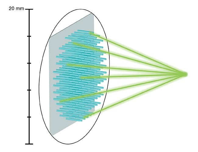
The current class of endoscopes requires high resolution in a compact form factor. Metalenses are a modern and increasingly popular solution to this and other requirements for designers. Courtesy of Ansys.
Several advanced technologies are driving the next generation of optical and optically enabled products. Freeform optics represent the first step beyond traditional lenses and mirrors, enabling higher levels of aberration control and light manipulation through additional degrees of freedom. Diffractive optics leverage the interaction of light with microstructures at wavelength scales to enable the creation of components that can precisely direct and disperse light for specific applications. And metasurfaces, which are constructed from nanoscopic, pillar-shaped building blocks called meta-atoms, placed on top of a dielectric surface, are on the cusp of redefining the interface between light and material, offering ultrathin yet powerful ways to control optical behavior.
In all cases, these pioneering technologies are critical in achieving the goal of miniaturization that is helping to reshape optical design, unlocking possibilities previously confined to the realm of science fiction.
Simulation in modern product design
It is often challenging to understand the right technology for an application as well as how to maximize the value of the technology within the design. Building physical prototypes can provide insight into some of these questions but is a costly and time-consuming option. This is especially true as designs incorporate more advanced technologies, such as freeform optics and/or metasurfaces.
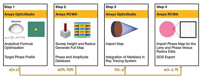
The multistep sequence shows the full design workflow for a metalens-based endoscope, with each step requiring different simulation software. Geometric ray tracing characterizes the desired performance of the metalens within the device; electromagnetic simulation characterizes the responses of meta-atoms, while the target phase and the meta-atom response is used to define an arrangement of meta-atoms that form the metasurfaces of the metalens and produce a layout for fabrication. The phase profile of the “real” metalens is sent back to ray tracing for validation; and a Graphic Design System (GDS) file for the metalens is created to enable manufacturing of the lens. Courtesy of Ansys.
Simulation enables engineers to subject their designs to a variety of scenarios, identifying weaknesses and optimizing designs before the first prototype takes physical form. This process is not merely about safeguarding against failure; it is an essential requirement for achieving the desired performance and reliability of an optical design.
Although advanced technologies are already established in helping to create smaller optics, they do not yet represent a complete solution for optical design. For example, while metasurfaces may be used to create an eye-tracking system in a virtual reality (VR) headset, macroscopic optical components, such as lenses and mirrors, are still needed for other parts of the headset design. Simulation must therefore be able to model systems that include optics at multiple scales, from microscopic to macroscopic.
Multiscale simulation must also be able to model the performance of those optics at full-system level, accounting for the effects of the real-world environment on the performance of the optics. For example, the introduction of “stray light” into the system, from unintended light sources, can have a significant effect on the system. And, for systems designed to produce images for human consumption, such as cameras or VR headsets, multiscale simulation must accurately model the response of the human eye to those images to simulate human vision.
Although multiscale simulation is an important starting point, the addition of multiphysics simulation is necessary to truly understand the performance of optics embedded inside of modern products. Through multiphysics simulation, designers achieve a better understanding of how the optics will perform when manufactured and integrated into a full product as well as how product performance will be affected by potential errors in the fabrication and assembly processes. Mechanical stresses introduced by the product packaging, or by thermal loads resulting from the presence of nearby electronics — and circulating airflows that may be introduced to mitigate those thermal loads — are additional variables for which multiphysics simulation can deliver key insights.
Simulation techniques and tools
Several techniques exist for optical simulation. On the macroscopic scale, geometric raytracing remains a reliable method for determining how light interacts with components such as lenses, mirrors, and prisms. While it is common to trace rays from the light source to one or more sensors in the system (forward ray tracing), it can be beneficial to instead trace rays from a sensor to the source. This approach (reverse ray tracing) is useful in cases in which the sensors are small, and it is computationally efficient to model the system in reverse.
Even at macroscopic scales, wave effects that are ignored by geometric ray tracing can be important considerations. As light comes to focus, or propagates through small but finite apertures, it will behave in a different manner than that described by rays. The behavior of light emitted from a coherent source, that then propagates over a long distance, will also be influenced by the wave nature of light. In these circumstances, techniques such as Fourier propagation and/or Gaussian beam decomposition can be used to model light.
As component sizes become smaller, electromagnetic simulation is often required to accurately characterize the performance of the optical system. Full solution(s) of Maxwell’s equations can be conducted using finite difference time domain (FDTD) or finite element method (FEM) simulation. In many cases, system properties enable simpler solutions. For example, when modeling diffractive optics or metasurfaces with regular
periodic structures, rigorous coupled wave analysis (RCWA) is often sufficiently accurate to characterize the performance of the component, even as the component is embedded in a larger system.
Engineers have the option to use several commercially available tools to perform optical simulations. Ansys, Synopsys, Lambda Research, and Photon Engineering are among some of the companies offering multiple solutions at the macroscopic scale. On the microscopic scale, Ansys, Synopsys, and Photon Design offer a suite of solutions.
There is also a push from smaller players to move simulation to the cloud, with offerings such as KostaCLOUD for ray tracing and Flexcompute for electromagnetic simulation. As the larger players in the industry begin to follow suit, the ability to conduct heavy computational workloads required for multiscale, multiphysics simulation across distributed compute clusters and graphical processing units will dramatically accelerate the optical design process. Distributed cloud computing is essential to enable multiscale, multiphysics simulation in a realistic time frame; such simulation requires significantly more computational resources than traditional single-scale, single-physics simulation. Therefore, it will be crucial for driving innovation in the next generation of optical and optically enabled products.
Design example: medical endoscope
The miniaturization of system design is key to the development of advanced medical diagnostics, in support of both invasive and noninvasive devices. For example, medical endoscopes have traditionally been limited in clinical applications by their relatively large size and low resolution. To improve performance and increase the use potential of these devices, metalenses are being considered in favor of macroscopic optics, such as ball lenses or gradient index lenses.
Metalenses, as well as freeform and diffractive elements, present a burgeoning optical technology. To harness their benefits, simulations must consider component and full-system variables. Courtesy of Ansys.
Developing a safe yet effective endoscope that includes metalenses requires rigorous design supported by multiscale, multiphysics simulation. The simulation workflow for such a design involves multiple steps. Geometric ray tracing is used to determine the required performance of the metalens inside of the macroscopic imaging system, as characterized by the phase of the light that passes through the metalens. An electromagnetic simulation tool (RCWA or FDTD) is used to characterize the responses of individual meta-atoms. Combining the target phase and the meta-atom response, simulation software creates an arrangement of meta-atoms that forms each metasurface of the metalens and produces a layout suitable for fabrication. The phase profile of the “real” metalens designed with electromagnetic simulation is sent back to ray tracing for validation, to ensure that the lens comprising real meta-atoms still meets system requirements.
Ray tracing analysis is conducted at both the subsystem level, including all the optics that make up the endoscopic imaging system, as well as at the full system level, to include the effect of external
factors, such as the light source for the endoscope and the device packaging. Iterations between the ray tracing and electromagnetic simulation tools may be required to achieve optimal performance of the system, especially when considering the effect of fabrication errors or unintended stray light. Once system performance has been validated,
a Graphic Design System (GDS) file for the metalens is created to enable the manufacturing of the lens.
Design example: aerospace and defense
In addition to the medical sector, multiscale, multiphysics simulation is essential to robust design in aerospace and defense. Systems developed for aerospace and
defense are mission-critical: These systems must perform accurately, and for long periods of time under operating conditions that are variable, and sometimes extreme.
Consider a high-speed aircraft used for surveillance or targeting applications. The high rates of speed at which this aircraft must travel will generate turbulence around the craft while atmospheric friction will induce nonuniform heating. This will result in asymmetric loads on the optical sensors that are difficult — if not impossible — to resolve via image processing electronics or software. Instead, the loads must be addressed within the design of the sensor itself.
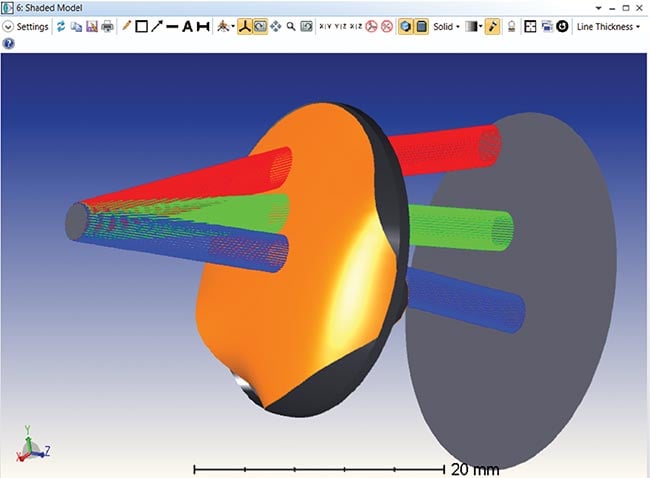
This model, capturing the design and simulation process, demonstrates how simulation is used to design a freeform optic that maximizes uniformity and efficiency across the field of view of an illumination system. Courtesy of Ansys.
The simulation workflow for such a design once again involves multiple steps. Geometric ray tracing is used to define the performance of the sensor under nontravel conditions. This analysis includes the effect of fabrication and assembly errors on the optical performance. Computer-aided design (CAD) tools, used to design the optical packaging, are coupled with ray tracing simulations to assess whether the packaging will generate unintended stray light in the combined optomechanical system. Computational fluid dynamics (CFD) simulations are run to calculate the flow fields surrounding the sensors. These nonhomogeneous flow fields affect the temperature and pressure loads on the optics and the refractive index of the surrounding medium. Further, the 3D refractive index profile of the surrounding medium must be accurately characterized to ensure proper performance of the system. This is especially important for the turbulent near-field region in front of the sensor, where the large variations in refractive index can lead to severe degradation of optical performance.
The optomechanical system, designed with geometric ray tracing and CAD tools, and the temperature and pressure loads, calculated from CFD, are passed on to finite element analysis (FEA) simulation to determine the structural displacements of, and 3D temperature distributions within, the optics. These results from FEA — along with the 3D refractive index profile of medium surrounding the sensor, calculated by CFD — are then brought back to the ray-tracing simulation for a full system-level validation.
It is often the case that the optics must be modified after incorporating the
effects of FEA. A simulation framework that supports automated workflows
between ray tracing, CAD, CFD, and
FEA by leveraging common material libraries and powerful application
programming interfaces is essential to enable dynamic optimization of the optics in a streamlined manner.
The future of simulation
In parallel with the development of techniques and algorithms in support of modeling modern optical technologies, advancements in computing technology are expanding the boundaries of what is possible with simulation. The ability to distribute massive computations in the cloud is a powerful means to enable faster simulation. Having real-time feedback on designs provides engineers with deeper insights into their optical designs, leading to the realization of more effective and innovative solutions.
And, as machine learning and artificial intelligence technologies mature, simulation will provide additional resources for engineers to gain added understanding of the systems they are developing and
how to improve them. For example, artificial intelligence can be used to define starting points for an optical design that the human designer may have not previously considered. This can in turn generate a new class of optical solutions for use in next-generation devices.
With more powerful and intuitive simulation tools, engineers are empowered to push the limits of optical design and ensure that the next generation of products exceeds the demands of tomorrow. The journey ahead is filled with opportunities to craft optical systems that are more efficient, more precise, and more apt to be integrated into daily life.
Meet the author
Sanjay Gangadhara is the senior program director for optics at Ansys. He works closely with the product management and R&D
leadership teams to define the long-term
product vision and business strategy for
the Ansys optics portfolio; email: [email protected].
/Buyers_Guide/Ansys_Inc/c32532