Using Lithography to Enhance LED Efficiency
Michael J. Lander
To increase the brightness of LEDs, the devices’ current-spreading layers can be synthesized from indium tin oxide instead of nickel and gold. Texturing the surface of the indium tin oxide layers can boost light output further. However, techniques used for patterning these top layers can deteriorate the diodes’ electrical properties, and they are hard to reproduce on an industrial scale. At the National Cheng Kung University in Tainan, Taiwan, researchers have created LEDs with a method that preserves layer integrity, that is low-cost and that could allow mass production.

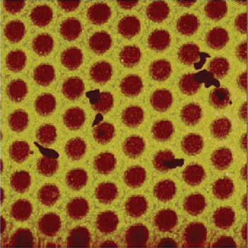
A scanning electron micrograph of a patterned LED shows 0.85-μm-diameter holes spaced 0.5 μm apart on its surface. Reprinted with permission of Applied Physics Letters.
As a surface for patterning, the researchers used 230-nm-thick indium tin oxide layers that were evaporated onto InGaN-based LEDs grown by metal organic chemical vapor deposition.
With a patterned hard mold, a high-pressure, high-heat molding process and chemical etching techniques, the scientists produced 1.75-μm holes spaced 1 μm apart in one sample. Using a different mold, they created another sample with holes of 0.85 μm and a spacing of 0.5 μm. They used atomic force microscopy to verify accurate pattern transfer.
Under a current of 20 mA, the forward voltages of the LEDs with large- and small-holed layers were found to be 3.25 and 3.24 V, respectively — close to the 3.24-V value measured for nontextured diodes. By comparison, previous photolithographic and dry-etching techniques resulted in increases of approximately 0.1 V, suggesting surface damage.
Output power for the diodes with 1.75-μm holes, as measured with a silicon photodetector, increased from 11.7 to 12.6 mW. In the layers with 0.85-μm holes, light output increased by 12 percent, attaining a value of 13.3 mW.
The light output advantage the system offers over LEDs with smooth indium tin oxide layers lies in the holes. Photons generated in the device’s multiquantum-well region scatter multiple times in the depressions, giving them a greater chance to exit. Because of the flat surface of conventional diodes, photons in them often are simply reflected back into the device at the substrate-air interface.
By optimizing the configuration of the pattern on the mold or by using a photonic crystal structure — research that they would like to conduct in the future — the researchers hope to improve the output power values. Although the method would be hard to implement because molds with submicron patterning are hard to find, the scientists say that the method could make micron and submicron lithography of LEDs significantly more economical.
Applied Physics Letters, July 2, 2007, Vol. 91, 013504.
Published: September 2007