Though the two terms above are often compared, one is a replacement strategy for pluggables while the other is a chiplet-based optical interconnect solution. A closer look at both will help clarify.
VLADIMIR STOJANOVIC, AYAR LABS
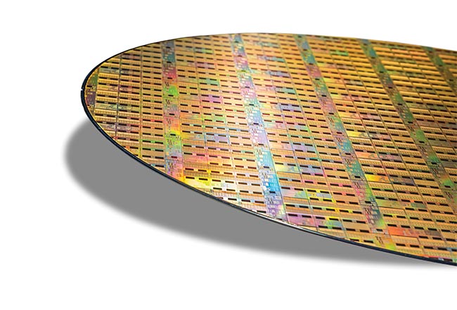
The use of traditional semiconductor fabrication techniques to create optical components on silicon wafers has opened the door to faster and more efficient solutions for high-speed data communication applications for data centers, artificial intelligence, high-performance computing, and other applications. Courtesy of Ayar Labs.
Recent advancements in silicon photonics are upending the optical market in the data center, with significant ramifications for how future AI, cloud, and high-performance computing systems will be designed, architected, and deployed. The core problem involves how to best connect compute chips over longer distances while maintaining bandwidth, energy, and density metrics that are acceptable for a given application.
At the same time, there is a lot of confusion — some inadvertent, some perhaps intentionally sown — regarding the differences between interconnect technologies such as co-packaged optics (CPOs), pluggables, and in-package optical I/O. Moreover, various industry standards are in play for these optical connections: What do they portend for the future?
Let’s start with some technology basics. For those unfamiliar with silicon photonics, it is a way to implement optical components in a silicon integrated circuit process, leveraging the semiconductor economies of scale to create photonic integrated circuits (PICs) that use light to transmit and process data. As with optical networking writ large, these PIC components can overcome many of the limitations of traditional copper-electrical connections to improve the bandwidth, latency, energy efficiency, and reach of signals within the data center.
Co-packaged versus in-package optics
How and where to use PICs for best effect in data center applications is where things start to get fuzzy, due to the various ways that the technology is packaged and implemented.
The current incumbent technology for connecting switches, routers, and servers in a data center is pluggable optical transceivers, which combines the PIC and other electronic chips into a module, roughly the size of a pack of gum. They provide board-to-board and rack-to-rack level connectivity and are used to easily insert and remove a fiber optic cable from a board faceplate, providing a connection between the electrical interconnects inside the board and optical fiber outside the board. Another benefit of pluggable optics is that the specifications of the transceiver inside the module can be tailored to the data rate and other requirements of a network architecture.
Though easy to maintain, pluggables will likely present problems with cost, power, bandwidth, footprint, and latency as data centers evolve to support more AI distributed-compute workloads.
One commonly proposed alternative to pluggables is CPO technology, which combines similar components from the pluggable (an electronic driver chip and a PIC) into a single package or module. This enables CPOs to have a smaller footprint and larger bandwidth density, which allows the CPO modules to be placed closer to the computer or switch chip package. This lowers the power of the electrical connection between the computer/switch chips and the CPO modules compared to the pluggables.
The other alternative is in-package optical I/O. As its name implies, in-package optical technology means that the optical interconnect, in the form of a chiplet that converts electrical signals into optical, is integrated into the same package as the chips used for compute functions (e.g., CPUs, GPUs, application-specific ICs, or field programmable gate arrays) (Figure 1). Optical I/O chiplets packaged in the same package as the compute or switch chips enable a reach-insensitive connectivity solution that is scalable in terms of fibers as well as connection throughputs. Optical I/O enables seamless communication across boards, racks, and compute rows, creating a distributed compute system at the bandwidth density, energy cost, and latency of in-package electrical interconnects.
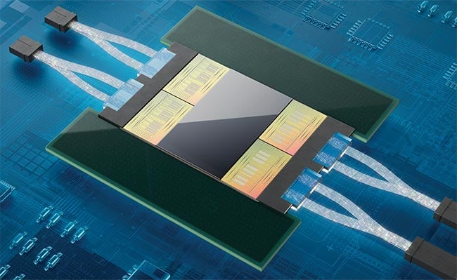
Figure 1. In-package optical I/O integrates optical interconnect into the same package as the chips used for compute functions. This approach enables chip-to-chip connectivity based on photons instead of electricity and, potentially, more efficient distributed compute systems. Courtesy of Ayar Labs.
At its most basic level, CPOs can be viewed as specifically geared toward data center networking, while in-package optical I/O is designed to create direct connections between chips at the board, rack, or system level.
Evolution versus revolution
Another way of looking at this is as an evolution versus a revolution. As mentioned, CPOs are a natural replacement — that is to say, an evolutionary step forward compared to the optical pluggables supporting networking systems inside the data center. These pluggable modules currently represent a massive market, and improvements in bandwidth density and efficiency are welcome and much needed.
In-package optical I/O, on the other hand, is an emerging revolution that addresses a new market. Specifically, the technology offers the low latency, high bandwidth, reach, and energy efficiency needed to enable new data center compute fabrics, such as memory-semantic fabrics, that are being tailored for machine learning scale-out, resource disaggregation, and memory pooling. Think of this as shifting the benefits of optical technology from the server and rack level to the board and chip level. It would allow massive collections of GPUs spread across the data center to operate as one at scale and communicate directly with disaggregated memory.
Powering all this interest, of course, is AI’s insatiable and growing hunger for more compute resources. Training these AI models requires linking thousands of GPUs (both for compute power and memory footprint) to enable next-generation data center infrastructure. For example, NVIDIA is expanding its NVLink memory-semantic fabric beyond its DGX servers, which normally host eight H100 GPUs. This directly connects up to 256 H100 GPUs into a group, using a two-stage NVLink fabric, with NVIDIA’s InfiniBand network used to connect more groups together. It is evident that this fabric scaling will continue, both in radix (i.e., the number of nodes supported) and bandwidth. As the market for AI progresses, it will require a solution such as optical I/O to facilitate the shift in fabric scaling — which is why industry players are investing heavily in in-package optics.
Inside in-package optical I/O
Although both CPOs and in-package optical I/O rely on silicon photonics techniques, one can see significant differences in their design when looking at the module level or deeper, in the case of in-package optical I/O chiplets.
These chiplets are fabricated in a CMOS process and assembled into monolithic 2D or 2.5D packaging that densely integrates them with transimpedance amplifiers, drivers, equalization, and control electronics as well as optical waveguides, modulators, and detectors. They support wide-parallel interfaces to allow in-package communications that are characterized by high bandwidth density and energy efficiency. To ensure interface compatibility, the market is coalescing around the Universal Chiplet Interconnect Express (UCIe) standard and NVLink-C2C. This standardization is critical for market success.
The optical links in these integrated chiplets are designed for optimal energy efficiency by exploiting parallelism — a common trait in CMOS chip designs that allows two or more operations to be executed simultaneously, each at lower speed but with double aggregate operation throughput. The chiplets use standard wavelength division multiplexing (WDM) enabled by the micro-ring resonators that selectively modulate and demodulate each of the multiple wavelengths per fiber (Figure 2). These photonic devices consist of an arrangement of mirrors and other elements that loop light waves back on themselves in a circle until a targeted wavelength is reached. Micro-rings are up to 1000× smaller than the optical devices in traditional Ethernet transceivers, which allows their integration on the same chip as the link electronics, and integration of multiple fiber connections on the same chip. Using these techniques, one current generation of chiplets achieved bidirectional throughputs of 4096 Gbps with eight optical ports (and 64 wavelengths).
Figure 2. Micro-ring resonators allow multiple wavelengths per fiber, and multiple fibers per chip. Courtesy of Ayar Labs.
Because energy efficiency is crucial for these applications, the chiplet uses wavelengths per fiber rather than increasing laser power and electronic rates to push higher data rates per wavelength. Throughput of data can thus scale by adding more wavelengths and optical ports without having to compromise energy efficiency.
Contrast this in-package optical I/O
approach with CPO modules, which do not integrate the optics in the same package as the switch or compute system-on-a-chip (SoC). A typical configuration might arrange 16 CPO modules, each in its own package, on an interposer board around a separately packaged switch. Though this approach might arguably be described more accurately as “near-package optics,” it is a form factor specified by the Co-Packaged Optics Collaboration Joint Development Forum and Optical Internetworking Forum (OIF).
Show me the data
Ultimately, it is these performance and efficiency characteristics of CPOs versus in-package optical I/O that will dictate where each fit in the market and why.
The first important comparison involves shoreline bandwidth density and energy efficiency (Figure 3). Chips, as well as the packaging for chips and boards, all have limited real estate along their edges, which is where data connection and heat dissipation occurs. Plotting out these various interfaces versus their reach capability illustrates the ability of a technology to move large amounts of data, at lower energy cost, over a given distance. Thus, it can offer a determination as to whether the package can be used to implement a distributed computing solution.
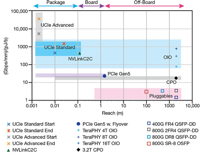
Figure 3. A product of shoreline bandwidth density and energy efficiency of various interconnect solutions plotted versus reach. Shoreline bandwidth density and energy efficiency relates to how efficiently a chip, board, or package uses the limited real estate for interface connections along its edge. Different interfaces also deliver different reach capabilities. Courtesy of Ayar Labs.
Applying the metric of bandwidth density (Gbps/mm) divided by energy efficiency (pJ/b) at the package level, the UCIe advanced interface with 2.5D integration offers the highest bandwidth/efficiency, but only across the span of a few millimeters.
The electrical UCIe Standard and NVLink-C2C connections are one step down in terms of density/efficiency, though they both offer slightly greater reach. Each can leverage standard organic substrates for in-package chip-to-chip connectivity. This reduces packaging cost(s) and these links offer both high shoreline bandwidth density and great energy efficiency, but unfortunately only over distances that limit them to within an SoC package.
Leveraging in-package optical I/O for these integrated connections allows the same bandwidth density and energy efficiency to extend anywhere in a large-scale distributed compute system — reaching up to hundreds of meters at least.
CPO technology is approximately an order of magnitude lower in this scale.
But, it offers more modularity over in-package designs, delivers reach that is greater than PCIe Gen5, and provides performance and density/efficiency benefits compared to current optical pluggables.
Another important metric is area bandwidth density (Gbps/mm2) and efficiency. Package real estate is at a premium for compute applications, which typically
use packages smaller than large networking switches. So, these packages need to efficiently use their limited area to host compute chips and memory stacks, which leaves little room for the I/O.
Area bandwidth density dictates how and where a packaging technique can be used in crowded rack and data center environments and settings. Figure 4
illustrates this spatial efficiency, showing in-package optical I/O in the neighborhood of electrical interconnect solutions, with CPOs closer to typical solutions used for networking.
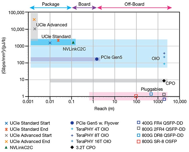
Figure 4. A product of area bandwidth density and energy efficiency of various interconnect solutions plotted versus reach. Courtesy of Ayar Labs.
Latency, the travel time of signals on
a network, is another important metric. Low latency, though critical for machine
learning scale-out and memory-semantic fabrics, is less vital for traditional networking applications. Simply put, poor latency is antithetical to the ability of chips to operate in parallel and communicate as a coherent whole with disaggregated memory. Ideally for such applications, latency should be comparable to current board-level copper-electrical connections. Low bit error rates (BERs) are critical for the same reason. Higher BERs increase the need for forward-error correction, which adds latency.
In-package optical I/O chiplets are
currently achieving 5-ns latency with
raw BER targets of 10−15. Current
CPO modules, like their pluggable
counterparts, require forward-error
correction to achieve such BER targets,
at a cost of 100 to 150 ns of latency in
the signal.
A final important metric is the cost efficiency of the interconnect solution, as measured by Gbps/dollar. Pluggable optics have generally failed to break the
1 Gbps/dollar barrier due to the number
of discrete components that they incorporate as well as their module assembly. At this point in time, CPO modules share similar issues. Though it is impossible to predict the future, it is logical to assume that CPOs will follow a similar cost trajectory as pluggables. Fortunately, this is not a hindrance in networking applications, because most of the cost is locked up in the switch. Also, many servers have relatively low throughput needs, and, thus, a low cost/Gbps requirement.
The situation is different for high-performance distributed compute,
since each compute unit (i.e., CPU, GPU, etc.) requires one to two orders of magnitude more off-package interconnect throughput to reach other parts of the
disaggregated/distributed architecture. Hence there is much greater focus on
in-package optical I/O solutions for the
substrate-level integration that has helped drive down costs with CMOS technology. This explains why recent design decisions favor electronic-photonic link integration on the same CMOS chip as well as integration of these chips into the same package as the compute SoC.
Hopefully these considerations explain why CPOs and in-package optical I/O
are exciting photonic breakthroughs, though for distinctly different applications. The characteristics differentiating each technology — performance per watt, power density, latency, package cost, and reach — dictate how and where they are suited for use in the data center, as well as where they fit in the silicon photonics market overall.
Meet the author
Vladimir Stojanovic, Ph.D., is chief technology officer at Ayar Labs. Prior to founding the company, he led the team that designed the world’s first processor to communicate using light. Stojanovic was one of the key developers of the Rambus high-speed link technology. He earned his doctorate from Stanford University; email: [email protected].