Perfect detection of long-wavelength IR radiation may be possible without cooling the photodetector.
Jozef Piotrowski, Vigo Systems SA
There is a common belief that it is necessary to cool long-wavelength IR photodetectors to achieve high sensitivity. The radiation is characterized by low photon energy; thus, detection requires electron transitions with threshold energy lower than the photon energy. At near room temperature, the thermal energy of charge carriers becomes comparable to the transition energy, resulting in a very high rate of thermal generation. The statistical nature of this process is the source of signal noise. As a result, long-wavelength detectors become very noisy when operated at near room temperature.
Cooling appears to be the direct, straightforward and most efficient way to suppress thermal generation. However, the need for cooling is a major limitation of photodetectors and inhibits more widespread application of IR technology. Affordable, high-performance IR systems require cost-effective detectors that operate without cooling or, at least, at temperatures compatible with long-life, low-power and low-cost coolers.
Because of the considerable cost, power consumption and inconvenience, it is desirable to eliminate or reduce the cooling requirements. A number of concepts to improve the performance of photodetectors operating at near room temperature have been proposed.1,2 This review examines approaches and technologies aimed at eliminating cooling requirements of IR photodetectors operating in the 3- to 8-μm (midwave IR) and 8- to 14-μm (long-wave IR) ranges.
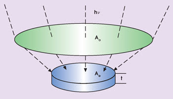
Figure 1. In this photodetector model, an absorber of IR radiation with physical area, Ae, and thickness, t, is coupled by an optical concentrator with its optical area, Ao, to the beam of IR radiation. One way to maximize detectivity is to maximize Ao/Ae.
Fundamental performance
Consider a generalized model of a photodetector, where the absorber of IR radiation (with physical area, Ae, and thickness, t) is coupled by an optical concentrator (with optical area Ao) to the beam of radiation (Figure 1). The detectivity of the thermal-generation-recombination limited device can be expressed as:

where η is the quantum efficiency and G and R are the volume generation rates.
As this expression shows, the detectivity can be improved by: 1) maximizing Ao/Ae using a concentrator of optical radiation (e.g., an immersion lens); 2) maximizing η/t1/2 with proper geometry of the device; and 3) minimizing G + R with a suitable selection of semiconductor material.
Consider optimization of the η/t1/2ratio. It can be shown that, for optimized thickness, this ratio is proportional to α1/2, where α is the absorption coefficient. The optimized thickness is 0.63/α for favorable conditions of double-pass IR radiation through the detector, with negligible and perfect reflection at front and back surfaces of the detector, respectively.
It is worth noting that the D* for the optimized detector is characterized by quantum efficiency of approximately 76 percent, reflecting a trade-off between requirements of a high quantum efficiency and a low total thermal generation. For the optimized device:

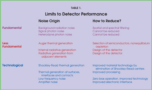
where Gα = G/α is the generation rate within the absorption depth per unity of area. Gα can be considered as the basic figure of merit of any semiconductor material for any type of IR photodetector. The ultimate background-limited photodetector performance (D*BLIP) can be achieved, with Gα reduced below optical generation caused by the background radiation (Table 1).
 Material systems
The most important material systems used for intrinsic photodetectors include binary narrow-gap semiconductors, tunable bandgap ternary semiconductors and bandgap-engineered superlattice materials (Table 2). The binary compounds can be used for applications that require optimum performance at the spectral range corresponding to the material’s bandgap. However, their availability is limited, and none can operate in the long-wave IR range.
Thermal generation and recombination in narrow-gap semiconductors at near room temperature will be determined by the Auger mechanism. Hg1–xCdxTe remains the champion material among a large variety of material systems. This is due mostly to the extreme flexibility of the material, which makes it possible to obtain a detector of any type for optimized detection within any region of the IR spectrum, including dual- and multicolor devices.
There is no clear indication that any well-known binary alloys and tunable bandgap semiconductors may be better than Hg1–xCdxTe in terms of the fundamental figure of merit. Consider, for example, the generation-recombination limited performance of approximately 5- and 10.6-μm-cutoff uncooled and thermoelectrically cooled Hg1–xCdxTe photodetectors (Figure 2). Optical immersion of the devices to GaAs hyperhemispherical lenses may increase the performance by an order of magnitude, bringing it closer to the background-limited photodetector limit.
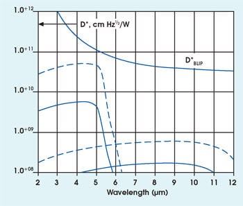
Figure 2. This graph of the generation-recombination-limited spectral detectivity of uncooled (solid) and two-stage Peltier-cooled (dashed) Hg1–×CdxTeHg1–×CdxTe photodetectors also indicates the background-limited-photodetector performance limit.
Some new materials may exhibit an improved figure of merit. An example is InNxSb1–x with a 15-μm cutoff.3 This is characterized by an Auger recombination rate, which is one-third that of equivalent bandgap Hg1–xCdxTe.
Intensive efforts are under way on artificial narrow-gap semiconductors based on type II and III superlattices.4 Researchers also have reported a reduction of the Auger generation rate at room temperature in InAs/GaAs superlattices that resulted in detectivity exceeding 108 cmHz1/2/W at 10.6 μm at room temperature.5 No devices of this type are commercially available at present.
Traditionally, photodetectors are related to photoconductors, photoelectromagnetic detectors and photovoltaic detectors, based on the principle that optically generated carriers in the absorber region are sensed. The recent advances in heterostructure devices made the distinction between photoconductors and photovoltaic detectors less clear, however.
Photovoltaic detectors
For a long time, photoconductors and photoelectromagnetic detectors were the only devices used for uncooled detection of mid- and long-wave IR radiation. Now they are being replaced by photovoltaic devices, which require neither electric nor magnetic bias, show no low-frequency noise and can operate from DC to very high frequencies. Photodiodes, with their very low power dissipation, can be assembled in large two-dimensional arrays.
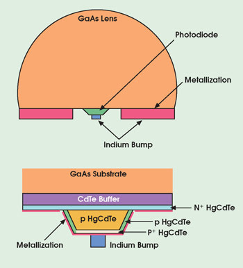
Figure 3. This schematic cross section of an optically immersed 10.6-μm mesa photodiode for operation at 200 to 300 K includes the complete structure (top), with an enlarged view of the active element (bottom).
An example of a mesa photodiode, monolithically integrated with immersion lenses, is shown in Figure 3. A heavily doped N+ layer provides the base contact with a low resistance. The top contact is a heavily doped P+-type layer covered with contact metallization that also acts as a retroreflector, inducing double-pass IR radiation. In practice, researchers use a more complex architecture with additional layers and a three-dimensional design to reduce G-R and tunnel currents generated at interfaces, surfaces and contacts.6
The thickness of the buffer and other layers within the device is frequently selected to achieve the optical resonance in a required spectral range. Optical immersion is often used to improve performance and reduce capacitance. The devices are fabricated with epitaxial techniques, such as isothermal vapor-phase epitaxy, molecular beam epitaxy, metallorganic chemical vapor deposition and their combinations.
The single-cell devices can be used successfully only for small-area uncooled and Peltier-cooled devices operating in the mid-IR. The long-wavelength photovoltaic devices operating at near room temperature suffer from poor quantum efficiency and low differential resistance.7
Because the absorption depth of long-wave IR radiation (>6 μm) is longer than the diffusion length, only a limited fraction of the photogenerated charge can contribute to the quantum efficiency. Take, for example, an uncooled 10.6-μm photodiode based upon Hg0.83Cd0.17Te absorbers. The ambipolar diffusion length in the material is less than 2 μm, while the absorption depth is approximately 13 μm. This reduces the quantum efficiency to near 15 percent for a single pass of radiation through the detector.
The resistance of the PN junction is very low because of high thermal generation and ambipolar effects. As a result, the noise from parasitic device resistance and the preamplifier may exceed the thermal generation-recombination noise. The two problems make the single-cell uncooled long-wave IR devices unusable in many applications.
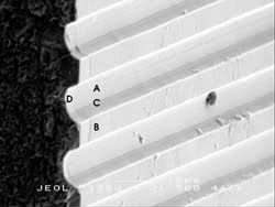
Figure 4. A scanning electron microscope image of a multiheterojunction photodetector illustrates the device’s mesa structure (A), trenches (B), and nonmetallized wall (C) and region (D).
These problems have been addressed by adopting sophisticated architectures with photovoltaic detectors based on multiple heterojunctions; for example, a device with junctions perpendicular to the surface (Figure 4). This is perhaps the only long-wave IR uncooled photovoltaic device on the market. Such devices can suffer from the nonuniform response across the active area and from polarization-dependent response.
More promising are solutions based on stacked multijunction photodiodes (Figure 5), which can achieve good quantum efficiency, large differential resistance and fast response.7 The problem in practical implementation is a low-resistance connection of N+ and P+ regions of adjacent cells in the device. This can be achieved by employing tunneling between the N+ and P+ interface in the engineered bandgap.

Figure 5. The back-side-illuminated multiple detector device with four stacked cells is supplied with a reflector for double-pass IR radiation.
Performance issues
The performance of photovoltaic devices operating at near room temperature has been improving steadily. Without optical immersion, photovoltaic detectors have subbackground-limited-photodetector performance that is close to the G-R limit. When thermoelectrically cooled with two-stage Peltier coolers, well-designed optically immersed devices can detect up to 1011 cmHz1/2/W at 5 μm, approaching the performance limit of background-limited photodetectors.8
The situation is less favorable for long-wave IR photovoltaic detectors. Detectivities exceeding 1 × 10⁹ cmHz1/2/W and roughly 6 3 109 cmHz1/2/W have been measured with uncooled 8.5-μm nonimmersed and optically immersed devices, respectively.1,2 Researchers have also reported optically immersed 10.6-μm photovoltaic detectors cooled with a two-stage Peltier cooler that can detect up to 4 × 10⁹ cmHz1/2/W.
Despite all these improvements (advanced architecture, optical immersion, Peltier cooling), they still show detectivities below the background-limited photodetector performance limit by almost an order of magnitude.
The frequency response of photovoltaic detectors is limited by the transport of photogenerated charge carriers through the absorber region and by the resistance-capacitance time constant. Transport through the absorber region is a combination of diffusion and drift. The p-type Hg1–xCdxTe is the material of choice for an absorber of a fast photodiode because of a large diffusion coefficient of electrons. The diffusion transit times are approximately 100 ps for an extrinsic, p-type, 2-μm-thick Hg0.82Cd0.18Te absorber. Further reductions are possible with a thinner absorber, and drift transport in reverse-biased devices can reduce the transit time.
The main limitation of response time is usually the resistance-capacitance time constant. In a transimpedance preamplifier with low input resistance, this constant is determined by the junction capacitance and the photodiode series resistance. Reduction of series resistance by almost two orders of magnitude is possible using structures with heavily doped N-type material for the mesa base layer, with corresponding reduction of the resistance-capacitance time constant.
A very short resistance-capacitance time constant is expected in optically immersed photodiodes with a very small active region. With these improvements, photodiodes can be used for gigahertz-range detection of IR radiation.
Auger suppression
So far, one of the most exciting events in the development of uncooled IR photodetectors has been the discovery of Auger suppression by British researchers.4,6 They proposed to suppress Auger processes and decrease the free carrier concentration below equilibrium values by stationary nonequilibrium depletion of semiconductors. This can be achieved in reverse biased N+pP+ photodiodes with a lightly doped absorber. Under strong depletion, the majority carrier concentration saturates at the extrinsic level, while the concentration of minority carriers is reduced below the extrinsic level.
The nonequilibrium mode of operation may reduce the Auger generation rate by a factor ni/Nd, where ni and Nd are the intrinsic and donor concentrations, with improvement of detectivity by (2ni/Nd)1/2. The additional gain factor of 21/2 is due to the negligible recombination rate in the depleted semiconductor. The gain for p-type material is even larger, taking into account the elimination of the Auger 1 and Auger 7 recombination. Additional depletion-related improvement can be expected from increased absorption resulting from the reduced band-filling effect.
The background-limited photodetector performance limit for a 10-μm device at room temperature can be achieved with:
• p-doping at a level of approximately 1013 cm–3.
• use of high-quality materials with a very low concentration of Shockley-Read centers.
• design of a device to prevent thermal generation at surfaces, interfaces and contacts.
Auger-suppressed heterostructural photodiodes have been demonstrated and gradually have improved, but they suffer from a large amount of low-frequency noise proportional to the bias current. Because the bias current of the long-wave IR devices is large, the 1/fknee frequencies are 100 MHz to a few megahertz for ≈10-μm devices at room temperature. This reduces their signal-to-noise ratio at frequencies of ≈1 kHz to levels below that for equilibrium devices.
The reason for the large 1/f noise is not clear. Using perimeter-area analysis to find its source provides, in part, contradictory results.9 The possible routes to decrease the 1/f noise include reducing the dark current and/or the In/I ratio with improved material technology and better device design.
Current status
Eliminating the need for cooling IR photodetectors will lead to logistical supply, a significant reduction in cost and an increase in the mean time between failures. It appears that there is no fundamental obstacle to perfecting detection of mid- and long-wave IR radiation without cryogenic cooling. The problems are of a technological rather than fundamental nature. The practical uncooled devices still present a challenge, but they have been steadily improved.
Where does the technology stand now? Thermoelectrically cooled and optically immersed mid-IR photodetectors closely approach the background-limited photodetector performance limit.
The best optically immersed equilibrium-mode long-wave IR devices cooled with two-stage Peltier coolers are an order of magnitude below that limit. The best nonimmersed Auger-suppressed long-wave IR devices also are an order of magnitude below the background limit of performance at frequencies above 1/fknee.
The performance of Auger-suppressed devices can be improved further by the use of optical immersion. Optical immersion also can significantly reduce the total bias power dissipation, which would be important in large elements and in future multielement arrays of extracted photodiodes. Another advantage is the significant reduction of radiative exchange between adjacent elements in an array. The combination of these improvements should lead to background-limited photodetector performance, with technologies currently available.
The photodetectors operating at near room temperature have found increasingly widespread civilian use in applications such as pyrometry and thermography; gas analysis with conventional, laser and Fourier transform spectroscopy; free-space high-transfer-rate optical communications; and test equipment. Military applications include night vision, laser rangefinders, threat warning devices, gun sights and smart munitions.
References
1. J. Piotrowski et al (2000). Uncooled photovoltaic Hg1–xCdxTe LWIR detectors. Proc. SPIE, 4130, pp. 175-184.
2. J. Piotrowski. Uncooled operation of IR photodetectors. OPTOELECTRONICS REV. (to be published).
3. N. Murdin et al (2001). Auger recombination in long-wavelength infrared InNxSb1–x. APPL. PHYS. LETT. 78, pp. 1568-1570.
4. A. Rogalski et al (2000). Narrow Gap Semiconductor Photodiodes. SPIE Press.
5. M. Razeghi. Type-II Superlattice Based IR Detectors. Web: cqd.ece.northwestern.edu/annualreport/038-39%20type%20II.pdf.
6. D. Maxey et al (Aug. 25, 1996). Growth of fully doped Hg1–xCdxTe heterostructures using a novel iodine doping source to achieve improved device performance at elevated temperatures. J. ELECTRON MAT., pp. 1276-1285.
7. J. Piotrowski et al (2003). Stacked multifunction photodetectors of long wavelength radiation. J. ELECTRON. MAT., 32, pp. 672-676.
8. IR Photodetectors, www.vigo.com.pl.
9. M.K. Ashby et al (2003). The 2003 US workshop on the physics and chemistry of II-VI materials. Extended Abstract, pp. 127-130.
Meet the author
Jozef Piotrowski is development manager at Vigo Systems SA in Warsaw, Poland. He is also an adviser at the Military Institute of Armament Technology in Zielonka, Poland; e-mail: [email protected].