A convergence of nanotechnologies and ultraviolet imaging is charting its course through the domain of optical microscopy.
NICOLAS LE THOMAS, GHENT UNIVERSITY-IMEC
Manipulating ultraviolet (UV) light beams is historically difficult and costly. As it relates to imaging, bulk optics in the UV range are expensive because they require unique materials, such as quartz, magnesium fluoride, or fused silica, to ensure aberration-free imaging with necessary degrees of focus and resolution. And, from a technical perspective, UV imaging
microscope objectives with a high
numerical aperture, which are required for high-resolution microscopy (operating below 360 nm), are rare. The high price tag that is typically associated with these objectives limits their use.
Courtesy of iStock.com/Digiphoto.
Increasingly, nanotechnologies are revolutionizing the usability of UV light across imaging applications. By integrating multiple optical components, including waveguides, modulators, and detectors — as well as their distinct functions — into a single chip, photonic integrated circuits (PICs) deliver precise control and manipulation of light from a compact design. For example, PICs may reduce the path length that light needs to travel for a particular application, reducing the chance of misalignment. PICs may also integrate customized waveguide designs that are tailored to a target wavelength.
Because standard semiconductor
manufacturing processes make PICs increasingly cost-effective and scalable
to high volumes, PICs are already well
established across a range of wavelengths in the visible and near-infrared. Now, PICs are drawing increased attention
for applications that harness the UV
spectrum. The precise control that PICs offer for beam shaping is critical for
optical UV microscopy, for example, in which the shorter UV wavelength compared to visible light enables interaction with comparably smaller structures and particles. Precise manipulation of the light beam ensures that it accurately focuses on the sample, thereby improving resolution.
In addition, PICs enable developers to build compact and cost-effective imaging systems. Such systems can be fabricated with more readily available materials compared to the legacy exotic materials on which traditional bulk optics rely, without compromising the optical properties in the UV range.
Ultraviolet capabilities
The arrival of nano- and integrated photonics technology into the UV band complements many important advantages that the properties of UV light offer for imaging applications. Indeed, the fundamental need for improved resolution and specificity has already driven the adoption of the UV wavelengths from ~200 to 400 nm for optical applications. The band is essential for probing subcellular structures and nanoscale material properties.
The UV spectrum is also critical for the observation of molecular interactions, because biomolecules exhibit a strong interaction with UV light. This quality increases the prospects of achieving favorable outcomes in many applications.
First, some amino acids, such as tryptophan and certain proteins, emit an auto-
fluorescent signal upon illumination, which enables label-free imaging. This is particularly useful for superresolution microscopy techniques, such as structured illumination microscopy (SIM), which has historically required the use of fluorescently labeled samples. At the same time, achieving label-free SIM does not discount the importance of UV light-sensitive fluorophores, which remain an important tool in microscopy and for life sciences imaging.
Further, a strong absorption in the UV wavelengths can significantly improve the Raman scattering process. This
occurs when incoming light interacts with a sample and generates scattered light at lower and higher energy and as a result enhances the signal-to-noise ratio. Investigations are ongoing into the use of UV light to overcome background noise in
on-chip Raman sensing applications.
UV waves also drive non-imaging
applications; in addition to biological and materials sensing and detection, which are used in pharmacology and materials research, UV waves are instrumental in quantum computing through ion trapping. In ion-trapped quantum computing, individual ions function as qubits to store and control quantum information. UV sources can generate the necessary electromagnetic fields to trap, cool, and manipulate ions with high precision.
Toward plug-and-play UV optics with PICs
For all their promise, the current class of commercially available PICs does not target the UV range. Laboratory demonstrations from the joint Ghent University-imec research team, however, have shown the efficacy of ultraviolet photonic integrated circuits (UV-PICs) — namely, UV-PICs that operate with low-loss single-mode waveguides at 360 nm1. In these laboratory demonstrations, single-mode waveguides allow only light with nearly identical properties, including wavelength and phase, to pass through. These components and the systems that they support, are essential for applications
such as UV-SIM where precise light
control is absolutely necessary.
SIM has previously been demonstrated in the far field as a traditional microscopy technique, allowing a user to look at a sample from a distance using bulk optics. PICs have previously been investigated in the near field, whereby the user looks very closely at the sample in the evanescent field. However, these near-field instances required the sample to be placed on top of the chip.
Recent research showed that the far-field SIM technique can also leverage the advantages of PICs, including in the UV wavelength range for label-free samples2. This advancement avoided inflicting any disturbance on the chip, which yielded a plug-and-play PIC element. In Figure 1, the sample is placed under the microscope. Here, the PIC is integrated into a conventional microscope setup, and it is used to shape the light beam in the far field.
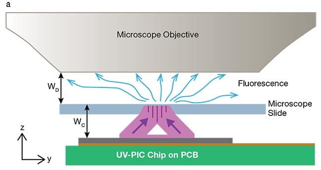
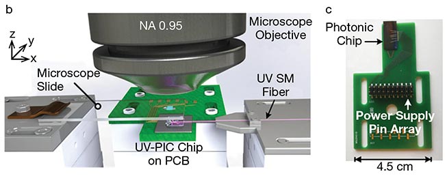
Figure 1. The compact ultraviolet photonic integrated circuit (UV-PIC) enables seamless integration into existing microscopy setups. A zoom-in on a sample area under the microscope with UV excitation light in violet and the fluorescent signal in blue (a). A schematic of the Ghent University-imec chip-based far-field structured illumination microscopy (SIM) setup, including a conventional microscope (b). The PIC mounted on an electric printed circuit board with wire connections (c). Courtesy of imec/Ghent University Photonics Research Group.
Reducing UV propagation losses
The Ghent University-imec team addressed the challenges of realizing low propagation losses in the UV, which presents a considerable challenge in UV chip-level operation. Many conventional optical materials used in PIC fabrication have higher absorption in the UV range. This means that a significant portion of the light is absorbed as it propagates through these materials, resulting in higher losses. In addition, waveguide surface structure is highly consequential at the nanoscale, with roughness causing scattering and the absorption of light. Because scattering losses scale as the reciprocal of the wavelength to the power of four, sidewall roughness also becomes a critical parameter in the UV. Further, the UV-transparent material must be compatible with standard semiconductor manufacturing processes to support the prospect of large-scale production.
Alumina, or aluminum oxide (AlOx),
is one promising option as a core waveguide material. It is compatible with large-scale manufacturing, and it theoretically has good optical transparency down to at least λ = 250 nm.
In its investigation of this material, the Ghent University-imec team showed that the high-temperature deposition of the AlOx layer via atomic layer deposition (ALD) coupled with an optimization of the etching process achieved propagation losses as low as 3 dB/cm at 360 nm in 800-nm-wide waveguides fully etched in 120-nm-thick AlOx layers, as shown in Figure 2.
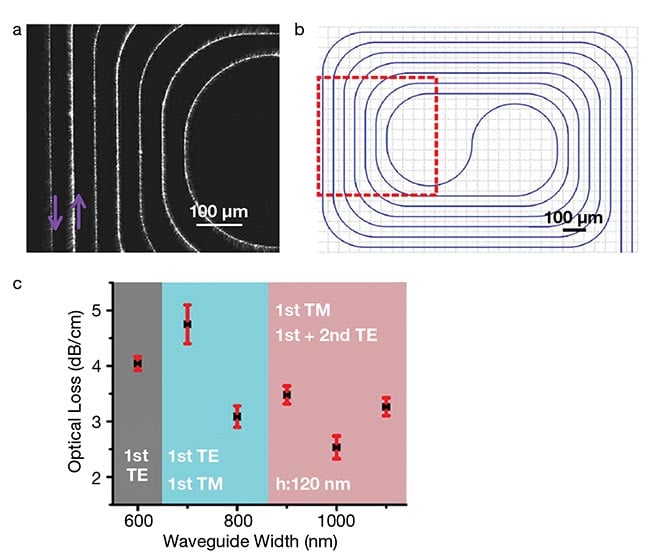
Figure 2. With 800-nm-wide waveguides fully etched in 120-nm-thick layers of aluminum oxide (AlOx), the researchers achieved scattering losses of only 3 dB/cm at 360 nm.
A microscopy image of the light scattering from a waveguide (λ = 360 nm) (a). The layout design of the waveguide corresponding to (a) (b).
The relationship between the propagation losses and the width of the AlOx waveguide; the different shaded areas correspond to an increasing number of possible guided modes (c). Courtesy of imec/Ghent University Photonics Research Group.
Breaking the field-of-view barrier
In tests, the developed UV-PIC enabled imaging of a field of view as large as 150 × 200 µm — a 22-fold improvement over the group’s previous work — and achieved an optical resolution enhancement factor of 1.84 compared to conventional visible light microscopy.
In combination with the UV-SIM technique, the researchers believe that the solution can be used to overcome
the impasse that exists between optical resolution and field of view: Increasing field of view means resolution losses,
and vice versa. In tests, the researchers used the design incorporated into the
SIM setup, in a label-free, far-field,
and wide-field (WF) configuration, to observe features in yeast cells that are otherwise invisible with standard WF microscopy.
Pushing boundaries
The study of large ensembles of bacteria or cells is a viable “killer application” for UV-SIM; incorporating PIC technology could further enable UV-SIM to provide similar benefits to flow cytometry for such study, for example. Traditional flow cytometry enables users to probe cells or particles, though only once. This inhibits users from charting the evolution of the same particle over time.
In contrast, with a vast field of view, a user could image up to hundreds of thousands of particles simultaneously and measure the evolution of seed cells or bacteria over time, and under various experimental conditions, such as upon the addition of nutrients or pharmacological substances. In addition, as UV light induces a strong autofluorescent signal, UV-SIM avoids the requirement of cell labeling.
Still, R&D advancements have not resolved all challenges. Photobleaching, which causes autofluorescence intensity to decrease gradually over time when exposed to light, thereby increases the amount of noise present in the final image and can reduce image quality.
Another microscopy approach, quantitative phase imaging (QPI), could be used to resolve this effect. QPI provides detailed information about cellular
morphology and dynamics without relying on fluorescence, and as a result provides high value for the study of live cells and tissues. Ultralow noise UV-QPI would bypass photobleaching and enable the imaging of bacteria or single-atom-thick monolayer materials, such as graphene.
Decreasing wavelength and chip sizes
The current iteration of laboratory-
demonstrated UV-PICs operates at
360 nm, exploiting the ultraviolet-C
(UV-C) range between 200 and 280 nm, and introduces a considerable range of potential applications. This is due to the stronger interaction of lower-wavelength UV light and biological molecules. imec is investigating new waveguide designs and the integration of low-loss materials, such as silicon oxide.
At the same time, the joint researchers aim to make increasingly compact PICs by integrating the UV light source on-chip. For 360-nm light, this includes the development of an ALD-AlOx platform on-chip for sensing and quantum applications. Additionally, in a collaborative European Union-funded initiative, the researchers will investigate transfer-printing aluminum gallium nitride sources on-chip.
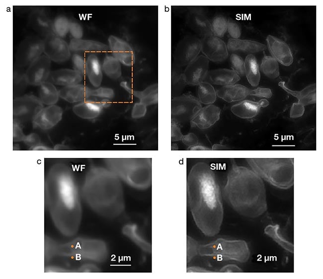
Figure 3. The ultraviolet photonic integrated circuit (UV-PIC) chip enables the observation
of features in yeast cells that are otherwise invisible with standard wide-field (WF)
microscopy. The images were obtained via structured illumination microscopy (SIM) in a label-free, far-field, and WF configuration.
Autofluorescence images of a coenzyme in yeast cells under UV-SIM and standard WF microscopy (a,b). Zoomed-in images of the
area delimited by the orange rectangle (c,d). Courtesy of imec/Ghent University Photonics Research Group.
At deep-UV wavelengths <280 nm, on the other hand, light beams possess even higher energy levels and will require specialized materials and manufacturing processes. Semiconductor UV-C lasers are at a very early stage, and further research is needed to increase the compactness of PICs for UV-C applications.
Meet the author
Nicolas Le Thomas is a professor in the
engineering faculty at Ghent University.
His main interests include on-chip high-
resolved microscopy, integrated photonic
sensors, biological applications of subwavelength photonic structures, optical spectroscopy of nanostructures, and semiconductor lasers; email: [email protected].
References
1. C. Lin et al. (2023). UV Photonic-
Integrated-Circuits-Based Structured
Illumination Microscopy With a Field of View Larger than 100 µm2. IEEE J Sel
Top in Quantum Electron, Vol. 29, No. 4, pp. 1-9.
2. C. Lin et al. (2022). UV photonic integrated circuits for far-field structured illumination autofluorescence microscopy. Nat Commun, Vol. 13, No. 1, p. 4360.