Compact ultraviolet lasers are finding growing applications in analytical measurement and materials processing, respectively, on either side of the 300-nm wavelength.
HANK HOGAN, CONTRIBUTING EDITOR
For compact UV lasers, advancements in technology and applications could make the sky the limit — literally.
When NASA’s Perseverance rover landed on Mars in February, for example, it carried a deep UV laser from Photon Systems as part of its scanning instrumentation. The metal-vapor laser enables the mapping of fluorescence emissions and Raman scatter from organics and minerals to support the rover’s search for traces of life.
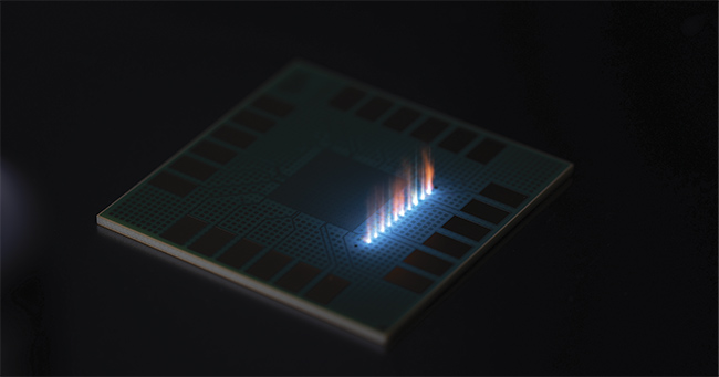
High-speed drilling and cutting of electronics using an 80-W UV hybrid fiber laser. Courtesy of MKS Instruments.
Photon Systems lasers use helium silver or neon copper as a lasing medium for emission at 224 and 248 nm, respectively. The latter technology was used on the Mars mission. Its emission is narrow
and stable, but due to beam-quality
limitations, the minimum focused spot size is only ~3 µm. At 100-mW peak power output, these quasi-CW lasers with 50-µs-wide pulses would not have the power necessary for materials processing, but they are viable for measurement applications.
Geoffrey Randolph, Photon Systems’ director of sales and marketing, said the company’s laser offered an important advantage to the Mars mission: The light that excites Raman emission in a material also causes fluorescence, which can
normally drown out the faint Raman
signal. But nothing fluoresces in the Raman emission zone just above the
248-nm laser wavelength. “Paradoxically, even though it’s a very short-wavelength laser, its Raman signal is fluorescence-free,” Randolph said.

NASA’s Perseverance rover landed on Mars in February, with a SHERLOC (Scanning Habitable Environments with Raman & Luminescence for Organics & Chemicals) instrument package mounted on its remote arm. This instrumentation relies, in part, on a 248-nm UV laser, which plays a key role in the search for signs of past or present life. Courtesy of NASA.
Of the two, fluorescence is a much more sensitive analytical tool, but Raman spectroscopy can more easily distinguish one substance from another. Combining the two techniques in one small, portable instrument helped to minimize the rover’s weight. But it could also be useful in manufacturing, environmental analysis, and public utilities.
Utilities in particular, Randolph said, are looking at direct reuse of treated wastewater, due to growing demand
and looming supply shortages. Such rapid reuse of wastewater requires a correspondingly fast method to determine whether any contaminants or pathogens are present. UV lasers could provide a means for doing so.
“Deep UV fluorescence and Raman potentially have the ability to analyze and discriminate pathological viruses and bacteria,” he said.
The UV lasers from Photon Systems and other suppliers make up a market that’s projected to grow at a compound annual growth rate of 8.31% between 2021 and 2027, according to an August 2021 survey from Market Reports World.
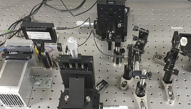
A 266-nm wavelength laser in a laboratory Raman spectroscopy setup. Compact deep UV lasers could enable lower-power and more portable systems for remote explosives detection. Courtesy of UVC Photonics.
Applications for these sources include materials processing and measurement, with a rough dividing line between applications and technologies at ~300 nm. Below this point, where laser power is typically lower, measurement applications dominate. Above this point, lasers offer higher power and can enable marking, drilling, cutting, and other increasingly important micromachining capabilities.
“As consumer electronics moves to smaller and smaller devices, as more things fit onto your phone, then UV lasers are becoming more important. The same thing is true in other spaces, like automotive and solar,” said Herman Chui, senior director of marketing at MKS Instruments.
Architectures and applications
MKS’s Light and Motion division makes a line of pulsed, continuous-wave (CW), and quasi-CW UV lasers. The latter category involves lasers that emit short bursts at repetition rates so high that, for practical purposes, they appear to be continuous wave because the time constants for an application are longer than the time between pulses, according to Chui. A representative example might involve a picosecond or femtosecond laser running at a repetition rate of 80 MHz or so.
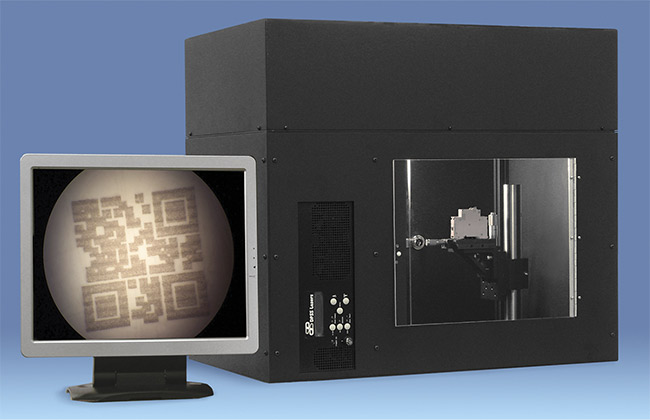
A quick response code marked on plastic by a UV laser system. Laser marking is among the largest application markets for DPSS Lasers’ UV systems in terms of volume and revenue. Courtesy of DPSS Lasers.
MKS Instruments’ UV laser centers
at around 349- to 355-nm wavelength emissions. The company’s lasers deliver up to 80-W single-mode average power.
Applied to UV-based micromachining, the technology offers advantages when drilling small, closely spaced holes or performing other tight-specification materials processing. For example, it allows a minimum focused spot size that scales down with wavelength. Additionally, most materials strongly absorb UV, which means the beam’s heat-affected zone tends to be smaller and shallower.
UV lasers may be the best way to micromachine the increasingly fine holes and features in printed circuit boards as onboard components continue to be more densely packed. A UV laser-based approach may also work better when machining emerging materials that offer improved electrical performance.
Chui said, however, that most UV lasers rely on the fundamental wavelength of infrared sources. Many of MKS Instruments’ systems use a near-IR diode to pump a neodymium- or ytterbium-doped crystal or fiber gain medium to generate 1000-nm light. Nonlinear optical crystals then convert this wavelength to its third harmonic, resulting in output wavelengths of 349 to 355 nm. Since these crystals incur conversion losses, the resulting
UV beam will have less output power than its infrared source.
Increasing conversion efficiency can improve the output power for UV lasers, and MKS is working toward that aim. The challenge is that there is usually a balancing act between improving laser conversion efficiency and maintaining crystal lifetime.
Alex Laymon, president of DPSS Lasers, also understands this challenge. The company makes diode-pumped solid-state lasers that use vanadate (vanadium yttrium tetraoxide, or YVO4) as the gain medium and lithium triborate crystals for frequency tripling to create a pulsed third-harmonic 355-nm output. DPSS Lasers does not manufacture UV systems that operate below 300 nm because doing so would decrease the product’s lifetime. The beta barium borate crystals required to quadruple the frequency to 266 nm cannot survive long enough when exposed to a flux of such high-energy photons, according to Laymon.
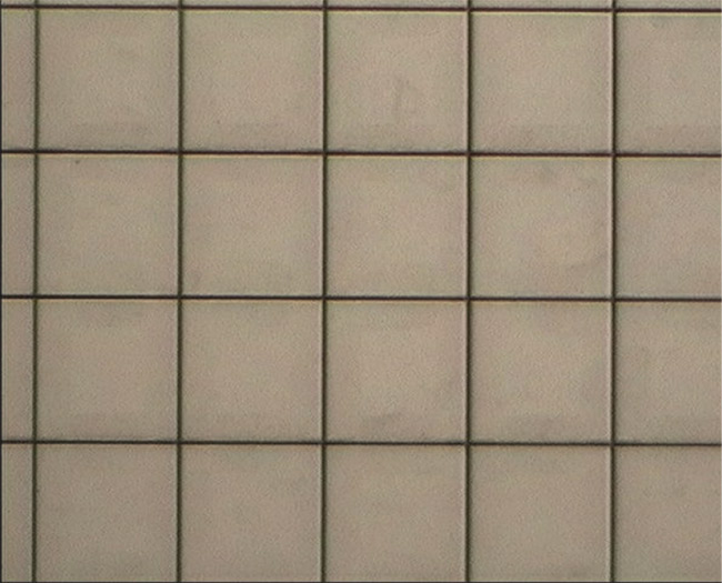
Sapphire scribed by a UV laser as part of a manufacturing process for blue LEDs. The square pads measure 300 µm on each side, and the scribe width is 10 µm. Courtesy of DPSS Lasers.
“UV lasers are more expensive than other laser systems,” he said. “There is no way to prevent this.” But he said the cost comes with benefits in key applications. Laser marking, for example, is the largest application for DPSS’s UV systems in terms of volume and revenue. Plastic curing, micromachining, and surface preparation also represent large markets.
Laymon predicted that longer lifetimes, smaller sizes, and price reductions would increase adoption of UV
lasers. He said these sources, however, will likely command only a small percentage of the market for laser systems.
Keeping crystals clear
Shorter-wavelength photons are more energetic, and so they interact more strongly with contaminants on any surface along the optical path. Contamination on the optics, such as an organic residue left over from a cleaning process, will absorb UV photons, undergo chemical changes, and then interact even more strongly with the high-energy UV photons. This can result in a runaway process that degrades the optics so much as to render them, and the entire system, unusable. So, rigorous protocols and designs are necessary to prevent photo contamination of UV optics, MKS Instruments’ Chui said.
Scott Buchter, CEO of UVC Photonics agreed, but added that both the energy and number of photons are important
considerations. His company’s lasers deliver only 10 mW of continuous power. Other lasers, such as those emitting above 300 nm for micromachining applications,
are pulsed systems that can emit peak powers in the tens of kilowatts. This translates into a lot of two-photon, damage-inducing absorption, he said.
But the manufacturing of systems that emit below the 300-nm wavelength also require contamination control. “Everything has to be clean,” Buchter said. “And you have to be careful how you clean.”
In January, UVC Photonics debuted a 261-nm CW laser that uses a praseodymium-doped gain medium pumped by a blue diode laser. The UV output arises from a second-harmonic generation of the 522-nm praseodymium emission.
During manufacturing of its system, UVC Photonics uses a jet of frozen CO2 (dry ice) for cleaning. The CO2 then evaporates, leaving nothing behind. The company then seals the systems and fills them with an inert gas. The system’s lower peak power and its highly controlled manufacturing process both help to minimize the impact of contamination on the product’s operation and lifetime.
Potential applications for UVC’s
261-nm laser include stand-off Raman spectroscopy systems for explosives
detection. Current versions of these systems fill a heavy backpack, but leveraging the UVC laser would enable a system small enough to fit in the footprint of a small, battery-operated device, Buchter said.
Other possible uses are in additional Raman spectroscopy applications, where UV lasers, in general, offer significantly higher sensitivity compared to commonly used IR lasers, Buchter said. He said a CW UV laser could also prove beneficial in microscopy, where light sources often need to deliver continuous low power.
As the list of current and potential applications grows for UV lasers, demand for the lasers will fuel continued progress in terms of their cost, size, and other parameters.