Using the right coating can improve detector sensitivity.
Glenn C. Tyrrell, Applied Scintillation Technologies Ltd.
Ultraviolet and vacuum UV detection and imaging sensors are required for scientific instrumentation — UV spectrometers and camera systems — used to evaluate the uniformity of beams in vacuum UV lithography equipment. Conventional CCD and CMOS devices are predominantly red-sensitive, peaking at ~800 nm.
General UVA, UVB and UVC applications require detectors that have responses in the 200 to 400 nm region of the spectrum. For semiconductor lithography applications, the wavelengths of interest are 193 and 157 nm and, in the future, wavelengths down to 13.5 nm will be needed for extreme-UV lithography (Figure 1).
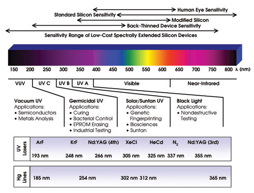
Figure 1. The wavelengths for detection depend on the application at hand.
The detector challenge
Conventional CCD and CMOS imaging devices and photodiode linear arrays cannot detect radiation in the UV region of the spectrum because of the high absorption of radiation in the surface of the sensor. Electrons are, therefore, not generated in the active part of the sensor. There are a number of solutions to the problem, including dedicated design and manufacture of detectors, and backthinning of conventional devices. These options can be expensive.
A cost-effective alternative is to produce spectrally shifted silicon devices by coating them with a suitable phosphor material that will be excited by the radiation of interest and that will emit in the visible region. Producing such detectors is a specialized process that requires detailed knowledge and understanding of phosphor down-conversion characteristics as well as the ability to produce a suitable coating. Key factors to consider are:
• Efficiency: absorbed photons/re-emitted photons.
• Excitation peak: wavelength of maximum absorption.
• Emission peak: wavelength of maximum emission.
• Decay time: brightness falling to 1 percent of maximum.
• Photostability: how efficiency degrades with exposure.
• Organic vs. inorganic luminescent materials.
• Phosphor particle size.
• Coating methods.
The ability to offer a commercial coating service to extend the capability of sensors benefits detector manufacturers by allowing off-the-shelf detectors to be rapidly adapted.
Phosphor types
Inorganic and organic phosphors are available. Lumogens are organic dyes that have been used for UV enhancement of conventional devices, particularly for imaging and spectroscopy applications. However, the coatings are not optimized for individual applications and are prone to degradation in higher intensity processes.
A unique organic phosphor developed by Applied Scintillation Technologies Ltd. for robust UV applications is Gorg. It is excited between 150 and 400 nm, with an emission peak at 545 nm.
Inorganic phosphors such as variants on divalent-europium (Eu2+)-activated barium magnesium aluminate (BaMgAl10O17:Eu, called BAM phosphors) also be can used in the 200- to 400-nm range. These phosphors are transparent above 450 nm. BAMb has an emission peak at 460 nm in the blue region of the visible spectrum (Figure 2), and BAMg has an emission peak in the green region. Figure 2 also shows the enhancement as a function of wavelength in the 260- to 400-nm region for a CCD array coated with BAMb or with Gorg. Both coatings flatten the response, suppressing the inherent device interference fringes between 320 and 400 nm.
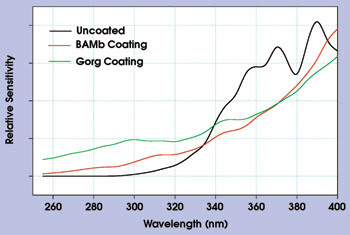
Figure 2. A Sony ILX 511 linear CCD array was coated with BAMb or with Gorg. Both coatings flatten the response.
None of these phosphors would be suitable for applications in the vacuum UV. Although Gorg does have some sensitivity between 150 and 200 nm, its decay time is in the millisecond range, which would make it unsuitable for applications requiring a fast decay. Inorganic phosphors for vacuum-UV applications have evolved from phosphors originally developed for x-ray and other applications. These include zinc and cadmium sulfides doped with silver, doped lanthanum oxysulfides and gadolinium oxysulfides (Gadox) doped with lanthanide elements.
The enormous range of energy levels in the lanthanides, such as terbium, praseodymium and europium (Tb, Pr and Eu), ensures that a phosphor with suitable excitation and emission peaks can be found for the appropriate application. In addition, x-ray and higher energy phosphors exhibit excellent radiation hardness and good photostability over time. Figure 3 shows the profile from a 193-nm laser operating at 10 Hz with a 1-ns, 1-μJ pulse obtained using a low-cost CCD custom-coated with a Gadox phosphor.
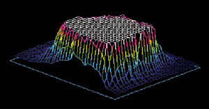
Figure 3. This profile was obtained using a CCD custom-coated with a Gadox phosphor. It shows a 193-nm laser operating at 10 Hz with a 1-ns, 1-μJ pulse.
Testing in a harsh environment
Phosphors for use in vacuum-UV and extreme-UV applications must perform well even after continued exposure to the radiation. Radiation-hard materials absorb as much of the incident energy as possible, protecting the device from damage. Gd2O2S:Tb, also known as P43, has been used in a variety of x-ray detector applications. Radiation hardness of the material has been evaluated using a synchrotron radiation source1, and phosphor coatings of various thicknesses and particle size have been evaluated for spatial resolution, light output and uniformity.2
The harsh extreme-UV environment also occurs in outer space, and the P43 phosphor also has been selected for use in detectors on the SWAP (Sun watcher using active pixel system detector and image processing) instrument3 that will be launched on the Proba-II technology demonstration platform by the European Space Agency in September 2007.
The instrument will obtain images of the solar corona — the upper atmosphere of the sun — to allow the detection of solar flares associated with the early phase of coronal mass injections. It will use an off-axis Ritchey-Chretien telescope to image the extreme-UV solar corona at 19.5 nm on a specifically fabricated extreme-UV sensitivity-enhanced (P43) CMOS active pixel detector. Extensive tests have been carried out on the scintillator efficiency at the Bessy synchrotron light-source facility in Berlin in preparation for the mission. This type of detector is expected to be highly useful for solar extreme-UV imaging.
Decay parameters
The decay time of the phosphor also can be a critical parameter and must be short for use with high-speed sensors. It must be shorter than the integration time, or else the phosphor will still be emitting light after the signal charge has been read from the pixel, resulting in smeared images. Some phosphors, such as Gd2O2S:Pr — which is becoming more popular for high-speed x-ray applications than Gd2O2S:Tb — exhibit a fast initial decay followed by an extended afterglow.
Scientists at Applied Scintillation Technologies have developed two methods that allow the acquisition of low-signal-level data from the afterglow.4 The techniques provide a much better understanding of the processes occurring in the phosphor, enabling refinements to be made. The first method, extended luminescence decay, enables measurement of the general fluorescence decay profile from nanoseconds to minutes, which results in a dynamic range of up to 10 orders of magnitude in the signal level. Because no single detector can linearly handle such a range, the experimental setup must be adjusted as the measurements are made.
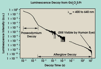
Figure 4. The extended luminescence decay data from a sample of Gd2O2S:Pr shows rapid decay up to 30 μs and a slower decay stretching out beyond 10 s — the afterglow.
The second technique, delayed photoluminescence spectroscopy, integrates all emission bands that make up the afterglow. The method is set up to eliminate the massive contribution from the initial decay. Gd2O2S:Pr has an emission spectrum whose major transition at 511 nm follows a logarithmic decay profile with a 7-μs decay time to the 10 percent level. However, there is a persistent afterglow that dominates the light output from 50 μs and that is visible to the naked eye in a darkened room for more than 20 s.
The scientists acquired extended luminescence-decay data from a sample of Gd2O2S:Pr (Figure 4). The curve shows two distinct decay characteristics: rapid decay up to 30 μs and a slower decay stretching out beyond 10 seconds — the afterglow. The afterglow fluorescence was measured using delayed photoluminescence spectroscopy (Figure 5). The slits to the monochromator used in the technique were set wide to accommodate the low light levels being sampled, giving a resolution of ~2 nm.
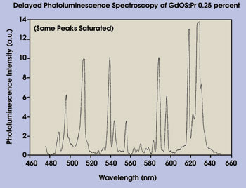
Figure 5. Photoluminescence spectroscopy was used to measure the afterglow fluorescence. The monochromator slits were set wide because of the low light levels, producing a resolution of ~2 nm.
The delayed photoluminescence spectroscopy of Gd2O2S:Pr (Figure 5) shows a number of peaks that do not appear in its normal photoluminescence but that exactly match the photoluminescence from Gd2O2S:Eu (Figure 6b), which also has a long afterglow. This shows that the Gd2O2S:Pr is, in fact, contaminated with europium.
Coating techniques
Considerable expertise is required to select an appropriate phosphor for a particular application, but once the phosphor has been selected, it must be coated onto the device. A number of factors must be considered when supplying a professional phosphor coating service:
• Removal and replacement of UV windows.
• Coating configuration (die or bonded device).
• Economies of scale.
• Risk assessment.
• Coating method.
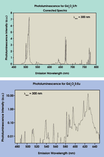
Figure 6. The photoluminescence spectrum of Gd2O2S:Pr (a) and the photoluminescence spectrum taken from a sample of a similar phosphor, Gd2O2S:Eu (b) are shown here.
Coating off-the-shelf devices may require the removal of a UV transmission window to allow access to the device surface, followed by the replacement with a new window after coating. The ability to do this should be part of the service offered.
Coating devices at the die stage is, in general, easier than coating finished ones because a finished device has the bond wires in place, and care must be taken not to damage or break the wires during coating. Given the above considerations, the coating provider must work closely with the device manufacturers to carry out a full risk assessment of the process.
Economies of scale also are important. Coating devices in batches or on a regular demand basis can be extremely cost-effective. “One off” coatings, especially for low-cost devices, can be prohibitively expensive, although for high-value devices, a suitable coating can provide real added value to the product.
At the heart of the process is the coating technique itself. The objective is to produce a uniform phosphor layer on the device surface that provides efficient down-conversion, protects the device from the effects of the incident radiation and offers good spatial resolution. One highly effective method is to apply a thin layer of “tacky,” optically transparent glue to the surface of the device and apply an excess of the phosphor in powder form. Blowing away the excess leaves a uniform layer of phosphor. The glue, which has been specifically developed for this application, can be spun onto the surface of the device or applied by a glue robot.
Using phosphor particles 4 μm in size gives a monolayer of 4-μm thickness. This provides more than adequate radiation protection for the device because the stopping distance for UV radiation is on the order of 2 μm. The inherent spatial resolution of the device is maintained, providing that each pixel contain at least one phosphor particle. Thus, this particle size works well on devices with pixels as small as 9 μm. Unlike coating methods in which the phosphor is deposited in an acrylic resin, this ensures that the radiation-facing surface of the phosphor layer does not have a covering either of glue or of binder and that the radiation enters directly into the phosphor material.
Choosing an appropriate phosphor and the optimum coating techniques enables the sensitivity of photodiode linear arrays, CMOS devices and CCDs into the extreme-UV range with significantly improved quantum efficiency.
Meet the author
Glenn Tyrrell is technical director at Applied Scintillation Technologies Ltd., Harlow, UK; e-mail: [email protected].
References
1. A.S. Tremsin et al (2001). X-ray-induced radiation damage in CsI, Gadox, Y2O2S and Y2O3 thin films. NUCLEAR INSTRUMENTS AND METHODS IN PHYSICS RESEARCH A, pp. 543-551.
2. M. Pokric and N.M. Allinson (2002). Testing of gadolinium oxy-sulphide phosphors for use in CCD-based X-ray detectors for macromolecular crystallography. NUCLEAR INSTRUMENTS AND METHODS IN PHYSICS RESEARCH A, pp. 353-359.
3. J-M. Defise et al (2004). Telescopes and Instrumentation for Solar Astrophysics. Proc SPIE, pp. 143-154.
4. J. Creasey and G.C. Tyrrell (2000). Rare-earth-doped materials and devices IV. Proc SPIE, pp.114-121.