What are quantum dots, and why are they important to today’s technology? Here’s a tutorial on the basics.
Sjoerd Hoogland, University of Toronto
It is hard to think about a life without semiconductor technology: The entire global information and communications infrastructure is based on semiconductors, and in every one of these applications, size matters. To create computer chips that operate at ever-increasing speeds, engineers must search for ways to decrease device size. One promising way of doing this is to replace electronic semiconductor devices with photonic ones, such as quantum dots.
Quantum dots exhibit unique characteristics, including size-tunability of their emission wavelength, an ultranarrow emission bandwidth, and a peak emission wavelength that is insensitive to temperature. These characteristics are tied to the fact that quantum dots exhibit discrete atomlike energy states because of the three-dimensional quantum confinement.
Quantum dots also can serve as the gain media in lasers, in which case the laser threshold is decreased dramatically compared with lasers with quantum confinement in fewer than three dimensions (e.g., quantum wells).
But what happens to the optical properties of semiconductors when their size is reduced to the scale of quantum dots? What confines carriers in all three dimensions, and what are the methods used today to accomplish this?
This article will address the most popular systems of epitaxially grown quantum dots, which have yielded lasers that are commercially available, and it will examine colloidal quantum dot nanocrystals synthesized chemically through the organo-metallic route.
Semiconductor properties
The crystal structure of a solid restricts the movement of carriers. In a semiconductor material, the outer electrons of the atoms are delocalized over the entire crystal, with the periodicity of the crystal structure limiting their movement. For a certain electron energy, the carrier is allowed to move in one direction, but its motion in a different direction is restricted as a result of destructive interaction from the atomic lattice. This dependence of the electron energy on the momentum of the carrier results in a structure of energy bands where the carrier can exist.
Semiconductors distinguish themselves from other materials by having an energy gap between the highest occupied energy band (the valence band) and the lowest unoccupied energy band (the conduction band). The bandgap of a semiconductor is measured between the top of the valence band and the bottom of the conduction band and is called direct if these extrema coincide in momentum (e.g., GaAs) and is called indirect if they do not (Si). Optical-emitting transitions are most likely to occur in direct-bandgap materials.
In the real world, the semiconductor crystal is finite, which puts restrictions on the allowed wave vectors within the energy bands, resulting in a set of discrete states available in each band with a wave vector separation determined by the size of the semiconductor.
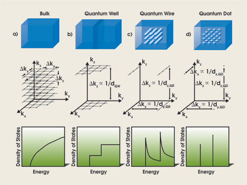
As a practical matter, the states in a macrosize chunk of semiconductor are so closely spaced that the conduction and valence bands appear to be continua. The number of these states per unit volume in an energy band is described by the density of states. Because no available states exist within the bandgap, the density of states is measured from the bottom of the conduction band and the top of the valence band from which it is, for a bulk semiconductor, a continuously increasing function with carrier energy (Figure 1a).

Figure 1. These graphics represent the active region (top), allowed states in momentum space (middle) and density of states (bottom) for confinement in no dimensions (i.e., bulk material) (a), in one dimension (i.e., a quantum well) (b), in two dimensions (i.e., a quantum wire) (c) and in three dimensions (i.e., a quantum dot) (d). (d = dimension(s) of quantum structure, k = momentum, QW = quantum well, QR = quantum wire, QD = quantum dot).
The magnitude is determined by the effective mass of the carrier, which is a measure of the degree of curvature of the energy band around the extrema — the larger the curvature, the smaller the effective mass of the carrier; the larger the wave vector separation between states, the smaller the density of states.
In semiconductors, electrons can be excited thermally to the conduction band, leaving holes in the valence band. Alternatively, electrons can be actively excited to the conduction band, for example, by absorbing a photon with energy larger than the semiconductor bandgap. The excited carriers will thermalize very quickly to the bottom of the conduction band (electrons) and to the top of the valence band (holes) by losing energy through carrier-carrier and carrier-phonon scattering.
The probability of finding an excited carrier at a certain energy in a semiconductor at thermal equilibrium is described by temperature-dependent Fermi-Dirac statistics. The overall carrier distribution in a semiconductor thus is a function of both the density of states and of the temperature-dependent Fermi-Dirac distribution. In a bulk semiconductor, this distribution is widespread, with a small number of carriers right near the edge of the conduction and valence bands and with a peak that is situated above (below) the conduction (valence) band, whose position is temperature-dependent.
Because the emission spectrum depends on the distribution and number of available transitions, a bulk semiconductor exhibits a temperature-sensitive emission spectrum, which is undesirable for stable lasing operation. Moreover, the temperature-dependent carrier distribution also makes the laser threshold temperature-dependent. These unfavorable optical properties of bulk semiconductors can be overcome by confining carriers to dimensions approximating the de Broglie wavelength of the carriers.
Toward artificial atoms
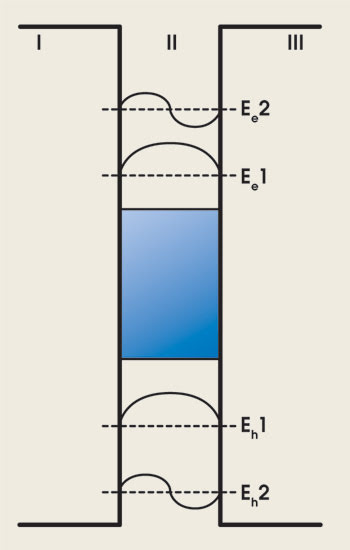
A quantum well can be formed by introducing a very thin layer of semiconductor whose bandgap is less than that of the surrounding semiconductor (Figure 2). Charge carriers in this potential well can survive only when their energies correspond to wave functions that satisfy the boundary conditions for a standing wave. Because these wave functions depend on the quantum well dimensions, the energies allowed in the well — and, hence, the effective bandgap — are tunable by adjusting the well dimensions. When the size of the well becomes comparable to the de Broglie wavelength of the carrier, the energy separation between the resonances becomes large enough to form a discrete energy spectrum.

Figure 2. Quantum confinement in a quantum well is realized by sandwiching a lower bandgap material (II) between two larger bandgap materials (I and III). A carrier is confined within the potential well when it has an energy of Ee1 or Ee2 for electrons and Eh1, Eh2 for holes. The wave functions of carriers at these allowed energies are standing waves, as shown.
The small width of the well results in the restriction of the carrier movement in the direction perpendicular to the well, causing the discrete energy spectrum. Because the width of the quantum well typically is several orders of magnitude smaller than the dimensions of the bulk semiconductor crystal, the wave vector separation between allowed states in the direction of the quantum well is greatly enlarged, compared with the bulk case (Figure 1a, middle). However, carrier movement parallel to the well is unrestricted, just as in bulk material, thus yielding a dense distribution of states in plane parallel to the well (Figure 1b, middle panel).
Therefore, at each allowed quantum-confined level, the overall density of states is determined by the wave vectors parallel to the well, thus yielding a two-dimensional density of states: At each allowed energy, a sharp increase of the density states occurs, as shown in the bottom panel of Figure 1b. This shape results in a less temperature-sensitive carrier distribution than in bulk material, with the peak emission wavelength more stable around the quantum-confined transition energies.
In addition, because of the increased number of carriers near the transition energy, the emitted light spectrum has a narrower bandwidth, the peak material gain is increased, and the transparency threshold is decreased.
All these improvements in the optical properties arise from quantum confinement of carriers in only one dimension. When taking the degree of confinement to the maximum by creating a quantum dot, the carriers are restricted in their motion in all three dimensions, eliminating the possibility of bulklike carrier motion. This leads to a truly discrete density of states exhibiting delta functions at the allowed energy states (Figure 1d). Such shape is analogous to atomic energy levels, and therefore quantum dots also are known as artificial atoms.
The number of charge carriers accumulated at the working transition is enlarged greatly at the expense of the higher-energy parasitic states of the continuum. Therefore, 3-D quantum confinement ensures not only temperature insensitivity of the emission wavelength but also the narrowest emission and gain bandwidths, as well as the lowest transparency threshold.
An excited electron and hole can interact with each other through Coulomb attractions, creating a quasiparticle called an exciton. How-ever, the binding energy required to create one is much smaller than the thermal energy; therefore, excitons have a very low probability of existing in a bulk semiconductor at room temperature. In quantum-confined systems, and particularly in a quantum dot, the excited electron and hole are forced to exist very close to each other, causing large Coulomb interactions between them. In this case, the binding energy and oscillator strengths are increased, and the excitons can exist at room temperature.
The degree of quantum confinement is determined by the interaction length over which the bond between an electron and a hole extends in an exciton, compared with the size of the quantum dot. In weak quantum confinement, the interaction length is shorter than the dimensions of the quantum dot, resulting in very closely spaced quantum-confined energy states. In this case, the quantum dot seems more bulklike because the electron and hole can separate beyond the exciton interaction length, thus breaking up the exciton and making the transition energy independent of the quantum dot size.
In the strong quantum-confinement regime, the quantum dot size is smaller than the electron hole interaction length, resulting in widely spaced energy states. The quantum dot sizes can be so small that the energy spacing between the allowed states in the conduction and valence bands is large enough to cause a so-called phonon bottleneck.
In most semiconductors, excited electrons can relax down to the bottom of the conduction band by losing energy through carrier-carrier and carrier-phonon interactions. However, a phonon bottleneck occurs when the spacing between energy states is much larger than these interaction energies — as is the case in strong quantum confinement. In this case, the probability for a carrier in a higher energetic state to lose its energy to a lower energetic state through these interactions becomes very low. As a result, electrons cannot relax to the bottom of the conduction band, and so quantum dots with strong quantum confinement should not be expected to emit light from the normal transition across the bandgap.
However, this phonon bottleneck has not been observed experimentally. This could be explained by the fact that fabricated quantum dots still are imperfect 3-D quantum-confined systems.
Epitaxially grown quantum dots
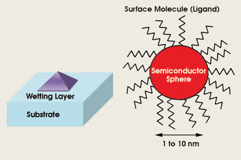
Epitaxial growth of one material on top of another with a different lattice constant causes strain. When this lattice mismatch is 5 to 10 percent, only several monolayers can survive the strain. Any additional layers are strained to the point that they break apart, forming islands of material on top of the surviving few monolayers. (The surviving monolayers are referred to as the “wetting” layer.)
This so-called Stranski-Krastanow growth method of self-assembled nanometer-size islands typically yields pyramid-shaped quantum dots with dimensions on the order of tens of nanometers for the base and several nanometers for the height (Figure 3a). The quantum dots’ small height allows for size-tunability of the bandgap, but their large asymmetry in shape results in an imperfect delta function-shaped density of states.

Figure 3. In a Stranski-Krastanow quantum dot, the strain caused by the large lattice mismatch between the substrate and the wetting layer material results in a contraction of the wetting layer material to form small islands, quantum dots (a). In a colloidal quantum dot, the core is a semiconductor sphere several nanometers across, with ligand molecules bound to its surface. The ligands typically contain long carbon chains to keep the dots in solution, to stop them from aggregating and to avoid any unsatisfied bonds of the surface atoms that could become trapping sites for excited carriers.
Because of its simplicity, the Stranski-Krastanow method is the one most often used to create quantum dots. The high crystalline quality that Stranski-Krastanow growth produces gives high radiative efficiencies, even at room temperature. However, the random nucleation of the quantum dots has a downside: There is limited control of the quantum dot’s size, so the emission spectrum of the ensemble is broader than the ultranarrow emission spectrum of a single quantum dot.
On the other hand, the large range of lattice mismatch allows for the growth of new material systems on common substrates. Emission from Stranski-Krastanow quantum dots has been realized from the near-infrared to more than 2 μm, while lasing operation has been demonstrated with ultralow thresholds and highly reduced temperature sensitivity of the emission wavelength. Commercial quantum dot lasers made from III-V semiconductor material systems now are available.
Colloidal quantum dots
Colloidal nanocrystal quantum dots are an attractive alternative to epitaxial self-assembled dots. They are chemically synthesized, typically through an organometallic reaction route without the need of ultrahigh-vacuum equipment or dangerous gases. They are suspended in an organic solvent so that they are castable from solution — for example, by spincoating — onto any substrate without lattice matching.
The synthesized spheroidal nanocrystal quantum dots remain in solution because the surfaces are passivated by organic molecules (Figure 3b), called ligands, which act as life preservers to keep the colloids in solution and to prevent them from aggregating. Unsatisfied bonds on the surface of semiconductors are sources for excited carriers to be trapped, resulting in a lower efficiency in the radiative recombination in the semiconductor. Binding the ligands on the surface of the colloidal quantum dots avoids such trap states by satisfying the unsatisfied bonds of the atoms on the surface of the colloids.
Typically, the size of the quantum dots is small (several nanometers) compared with the exciton radius (several tens of nanometers), ensuring strong confinement of carriers and enabling bandgap tunability by varying the size of the dot. The concentration of the reaction chemicals, the reaction temperature and the duration of the reaction determine the final size of the colloids, with a size distribution of typically less than 10 percent.
Postsynthesis, the ligands can be replaced with molecules that have specific end groups that serve a particular purpose, such as binding the colloids to specific molecular species to use the emissive dots as biological markers.
Some colloid material systems also can be overcoated by a different semiconductor material that has properties to improve surface passivation. In addition, careful choice of the overcoating material and its thickness could alter the electron and hole interaction strength; for example, to optimize the carrier density to obtain a population inversion.
The true strong confinement regime ensures large separation between allowed energy levels, but the small size distribution gives rise to a continuous absorption spectrum in which only the lowest allowed transitions are clearly observable. The energy separation between allowed states for these types of quantum dots is very large compared with the phonon energies, but no phonon bottleneck has been observed. The most widely used colloidal quantum dots consist of II-VI semiconductors, where cadmium-based materials provide operation in the visible spectrum and lead-chalcogenides in the near-infrared.
Meet the author
Sjoerd Hoogland works for a privately held venture and was a postdoctoral fellow at the University of Toronto when he prepared this article; e-mail: [email protected].