
Test Design Kits Accelerate a ‘Fab-less to Lab-less’ Transition
Limited by legacy test practices amid a ramp-up of photonic integrated circuit production, engineers are turning to test design kits to bridge the gap.
CHIARA ALESSANDRI, LUCEDA PHOTONICS, AND BEIBEI WU, JFS LABORATORY, CHINA
Increased demand for datacom transceivers and a surge of applications that rely on AI and quantum technology have combined to drive significant growth in integrated photonics. Market research published this spring by IDTechX now values the photonic integrated circuits (PICs) market at more than $20 billion by 2034. As the sector experiences robust advancement in its technologies and markets, this current value indicates only a portion of the potential that integrated photonics appears to be capable of realizing.
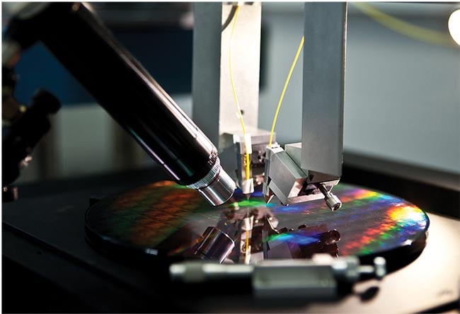
By offering test design kits (TDKs), test engineers provide their design engineer partners with easy access to their test capabilities and ensure that their chips are testable using automated die-level and wafer-level testing routines. Courtesy of Ghent University-imec.
For all the promise that market projections offer, forecasts such as these fail to focus on existing challenges that must be met to ensure that integrated photonics maintains and builds on its current momentum. One of the greatest hurdles that currently faces the industry is testing. As the production of photonic chips continues to increase, current test practices, as well as necessary infrastructure, do not scale effectively.
There is more to overcoming this bottleneck than simply identifying it: Testing for PICs is inherently complex, requiring more than sophisticated equipment. It demands extensive know-how in the calibration of this equipment, plus PIC chip design, thermal and polarization control, and high-speed measurements. These requirements demand a depth of expertise held by only a handful of specialists.
In addition, many companies, R&D centers, and academic institutions are unable to afford in-house test equipment, which requires a substantial economic investment to purchase and a skilled workforce to operate. The difficulty in developing and accessing testing knowledge and equipment hinders production scale-up. This emphasizes the need for a more dynamic and accessible testing framework within the industry as well as for standardization.
Test as a service
The concept of testing as a service has been growing steadily in the integrated photonics sector, with momentum both from industry and within foundries, which are beginning to offer complementary test services in addition to their fabrication services. This trend is gradually transforming the landscape by making advanced testing capabilities accessible to a broader range of companies, R&D centers, and academic institutions.
However, a significant challenge persists: The complexity of determining the yield of wafers is often compounded by the fact that many designs are not optimized for testing.
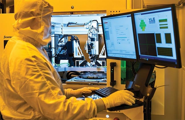
Test engineers conduct measurements of PICs on wafer-level testing platforms. These engineers benefit from early-stage alignment with design engineers to understand the necessary equipment and parameters to optimize testing. Courtesy of VLC Photonics.
“We often receive wafers and chips that are difficult or even impossible to measure using our standard equipment configurations,” said Iñigo Artundo, CEO of VLC Photonics, a design and testing house in Valencia, Spain. “As a result, the biggest challenge becomes developing custom test setup configurations to adapt to layouts that are not properly conceived in the first place.”
This mismatch causes delays, reduced throughput, and intensifies the need for manual intervention. The ultimate result is an increase in nonrecurring engineering costs and time investments for stakeholders spanning test providers to end users.
Bridging the gap between design engineers and test engineers is essential to address these challenges. Test providers must create an environment in which design engineers have a thorough understanding of the boundary conditions and limitations of test equipment. At the same time, receiving detailed test plans from designers early in the design phase will benefit the testing process by ensuring that test engineers can swiftly adapt the necessary equipment.
Design for test
Design for test (DfT) involves designing circuits while proactively accounting for test requirements and restrictions from the outset of the design stage. Correct placement of optical and electrical I/Os on the chip, considering compatibility with test equipment and methodologies, is critical to enabling engineers downstream to effectively test the designed circuits. A well-structured test protocol further improves the chances of an efficient transition from the design phase into the testing stage.

Light is coupled into a PIC through an edge coupler: a common means for coupling light in and out of the chip while offering a large operating bandwidth. Courtesy of VLC Photonics.
The concept of DfT also covers steps to improve testability and understand
circuit performance. For example, strategically placing monitor points on functional circuits — implemented by adding unused ports or power taps distinct from the primary product I/O interfaces — provides essential information about the circuit during R&D and early production.
“These monitor points facilitate the analysis of the circuit behavior, making it possible to isolate failures,” said Chris Barnard, senior director of silicon photonics engineering at OpenLight Photonics, a designer and manufacturer of silicon PICs. “If we measure a high loss between two monitor photodiodes, with several components in between, it becomes impossible to pinpoint which component is causing the loss without adding additional test ports.”
Similarly, adding component and subcircuit test structures on the chip can lead to a better understanding of the measurement results, and help engineers debug critical parts of the design. This practice leads to faster iterative design improvements. “Adding debug structures to the layout that can include probing individual circuit blocks or components within the larger PIC is crucial,” said Amit Dikshit,
design enablement manager at AIM Photonics. “These structures can identify the ‘smoking gun’ when the PIC does not perform as expected.”
Implementing these DfT hallmarks in a design can pose a challenge, especially given the need to balance the requirements of foundries and testing partners. Adherence to design rules ensures manufacturability and compatibility with established, consistent testing methodologies. It is necessary to integrate these rules into the software that engineers use to design and simulate their circuits.
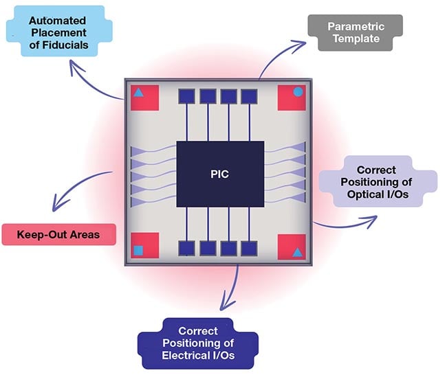
Common test design kit (TDK) features include the automated placement of fiducial markers as well as the definition of “keep-out” areas based on the physical constraints of the measurement equipment. In this way, TDKs provide a set of layout guidelines that can be used to optimize test-stage processes. Courtesy of Luceda Photonics.
Design software dedicated to the layout and simulation of PICs offers advanced simulation capabilities that allow designers to predict test outcomes and accordingly refine designs. Meanwhile, features such as advanced place-and-route, functional verification, circuit simulation, and model extraction enable the design of clever test structures. Collectively, these considerations offer insight into how test providers may leverage design platforms to align the needs of both test and design engineers.
Test design kits
Foundries enable designers to adhere to their specific fabrication rules by offering process design kits (PDKs) that are compatible with PIC design software platforms. These kits intermediate designers and foundries, democratizing access to manufacturing facilities and ensuring that foundries can easily ramp up production.
This methodology can be similarly transferred to the testing regime, where the development of test design kits (TDKs) compatible with PIC design software effectively facilitates the design-for-test process. In fact, the strength of TDKs is in their orthogonality to PDKs: Both types of design kits can be used simultaneously by designers, creating an environment in which test providers can easily support the testing of any chips coming from any foundries, without needing to know what PDK customers are using.
In this way, TDKs represent an important pathway to a scale-up solution by streamlining communication opportunities between test providers and end users.
TDKs also raise awareness about the importance of testing early on, ensuring that adequate funds are allocated just as they are for design and fabrication.
“As a design house, we always advise our clients to start with the end in mind,” said Kevin McComber, CEO of PIC design services and software firm Spark Photonics. “But even when they do, trying to design using specifications from a written document is time-consuming and prone to errors. Using a TDK solves those issues as there is very little room for ambiguity.”
Broadly, TDKs are valuable at any reach on the photonics value chain, serving to reduce the cost barrier and total time required to get chips measured. “This is true for low- and mid-volumes across multiple customers as well as large volumes from individual customers,” said Sylwester Latkowski, scientific director at Netherlands-based Photonic Integration Technology Center. “Well-structured test protocols and layout designs enable monitoring of product manufacturing through different stages, understanding the bottlenecks, optimizing the production windows, and overall yield.”
Peeling back the layers on TDKs
TDKs provide design rules and layout guidelines that allow engineers and end users alike to correctly position the circuit I/O ports, both optical and electrical, on the die design. These kits embed automated rule checks for real-time feedback during the PIC layout preparation, enabling a sequential design flow. The initial design can be virtually evaluated, corrected, and retested iteratively until the completion of the final test-ready design.
According to Siyang Liu at Wuhan, China-based JFS Laboratory, by incorporating features required to test successfully, TDKs — and the tests that they enable — prevent situations in which testing becomes partially or completely unavailable. When measuring photonic chips using fiber arrays, for example, it is necessary to include fiber loopbacks in the design. Rather than manually providing feedback to designers through graphic design system (GDS) and PDF files, test providers can count on TDKs to automatically add loopback structures to the customer’s design, minimizing the chance of human error.
There are many other examples of TDK features, including the automated placement of fiducial markers and the definition of “keep-out” areas based on the physical constraints of the measurement equipment. The correct positioning of optical and electrical I/Os, in terms of pitch between the ports, their orientation, and/or their absolute position on the chip, is another possible feature. TDKs may also integrate a device labeling system to support automated wafer-level testing.
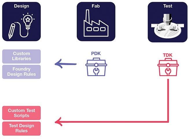
Test design kits (TDKs) facilitate the design-for-test process, providing access to test routines and design rules early in the design process. Courtesy of Luceda Photonics.
After a design is completed, TDKs use existing software features to generate the outputs needed by test providers to perform tests. These outputs include the GDS file of the design. Another important output is a list of components and their connectivity. Each individual component is assigned a name, number, and key
parameters so that test providers can
easily identify it when initiating the test routine. Fiber grating couplers, for example, which are commonly used as optical I/O interfaces for PICs, are characterized by the vertical coupling angle, which affects their testability. Test providers working with these components must know the value of this angle to position optical fibers to ensure the maximum coupling of light into the waveguides on the chip. Structurally accessing such information is crucial for test providers to speed up the testing process.
It is also necessary to optimize the extraction of the positions of both electrical and optical I/Os on the die or wafer. Although the extraction algorithms are embedded in the design software, each TDK outputs this information in a format that is compatible with the measurement software and tools used by each test provider, or with each test routine if multiple tools are available.
TDKs can go even further: Imagine a virtual environment that allows designers to test their circuits in a digital space
exactly as they will be tested under regular physical parameters. Design software can offer an ideal digital space, while test partners provide real space. TDKs interface between the two. Running simulations on the PICs beforehand allows designers to validate the testability of circuits, identify the measurement parameters needed to characterize a specific device or circuit, and estimate the test time.
Such an approach enables design engineers to check which test probes are supported by the test provider, and whether the test equipment capabilities allow measurements within the voltage or wavelength range needed to characterize a specific circuit. If, for example, the test equipment for the high-frequency testing of transceivers for datacom applications
supports measurements of up to 50 GHz,
but the customer needs to measure responsivity of up to 100 GHz, it is crucial for the test provider to know this requirement in advance to avoid delays. Similarly, measurements of nonlinear effects in a device may require laser powers higher than those which are supported by the available equipment.
Finally, users can align the output file format of such simulation jobs with the output format of the measurement routines, customized per TDK. This way, test providers can provide designers with a straightforward way to compare simulation and measurement data within the design software environment. This automation reduces the time required for data analysis and ensures that all test data is accurately recorded and reported.
Scaling test to industry
The broad adoption of TDKs is poised to revolutionize the PIC industry by enabling more complex designs with guaranteed testability, thereby improving
standardization. This will improve
efficiency and reliability and is critical
to bolster the competitiveness of the integrated photonics industry as heterogeneous integration and advanced chiplet architectures emerge as demand for PICs increases.
TDKs most critically encourage designers to view testing as an integral part of the design process rather than an afterthought, by providing parametric test templates, design rules, and layout guidelines. This shift in mindset reduces engineering costs for both designers and test providers. At the same time, it accelerates the time-to-market for photonics-powered products.
There is one additional advantage: TDKs facilitate developing trained members of the workforce for software-assisted wafer-level characterization. This serves as a necessary assurance that the industry has the talent it needs to continue innovating and growing.
Meet the authors
Chiara Alessandri is product marketing and technical sales manager at Luceda Photonics. She oversees market research, positioning, and messaging efforts, and works with ecosystem partners and in customer collaboration for the design software and services provider; email: [email protected].
Beibei Wu is a senior engineer of silicon photonics at JFS Laboratory. She previously worked in silicon photonics/lidar R&D at Chongqing United Micro-Electronics
Center. She received her doctorate in optical engineering from Huazhong University of Science and Technology; email: [email protected].
/Buyers_Guide/Luceda_Photonics/c32297
Published: September 2024
Glossary
- semiconductor
- A semiconductor is a type of material that has electrical conductivity between that of a conductor and an insulator. In other words, semiconductors have properties that are intermediate between metals (good conductors of electricity) and insulators (poor conductors of electricity). The conductivity of a semiconductor can be controlled and modified by factors such as temperature, impurities, or an applied electric field.
The most common semiconductors are crystalline solids, and they are...
- integrated photonics
- Integrated photonics is a field of study and technology that involves the integration of optical components, such as lasers, modulators, detectors, and waveguides, on a single chip or substrate. The goal of integrated photonics is to miniaturize and consolidate optical elements in a manner similar to the integration of electronic components on a microchip in traditional integrated circuits.
Key aspects of integrated photonics include:
Miniaturization: Integrated photonics aims to...
- integrated optics
- A thin-film device containing miniature optical components connected via optical waveguides on a transparent dielectric substrate, whose lenses, detectors, filters, couplers and so forth perform operations analogous to those of integrated electronic circuits for switching, communications and logic.
- photonic integrated circuit
- A photonic integrated circuit (PIC) is a compact and integrated device that incorporates multiple photonic components and functions on a single chip, similar to the way electronic integrated circuits (ICs) integrate various electronic components. The goal of a photonic integrated circuit is to manipulate and control light signals for applications in optical communication, sensing, signal processing, and other photonic technologies.
Key points about photonic integrated circuits:
Integration...
FeaturesLuceda PhotonicsdesignPICssemiconductorindustrydesign for testintegrated photonicsintegrated opticsprocess design kitsphotonic integrated circuitphotonic integrated circuits