Suspended Nanotubes Imaged by Photoluminescence
Daniel S. Burgess
The luminescent response of optically pumped single-walled carbon nanotubes may be used to create images of the structures, report scientists from the Institute for Microstructural Sciences in Ottawa and from the University of Ottawa. Employed as a nondestructive imaging modality, photoluminescence offers a means of locating nanotubes for assembly into optoelectronic components and of exploring fundamental characteristics of the structures, they suggest.
New means of observing nanotubes suspended in air over trenches in a substrate are of particular interest, they propose, because the objects display potentially useful optoelectronic characteristics, having been used to construct basic emitters and detectors in recent years. The problem is that existing imaging techniques can be too invasive. Scanning electron microscopes, for example, can damage the tubes or leave behind deposits that prevent luminescence, and confocal microscopy can generate optical power densities sufficient to knock the tubes off their perches across a trench.

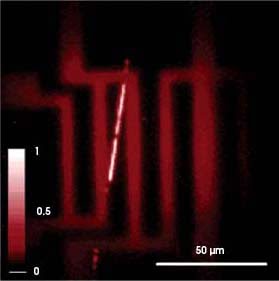
The near-IR photoluminescence from a 100-μm-long single-walled carbon nanotube (white) is used to create an image of the structure, which is suspended over a series of partially filled trenches (black) in a silicon substrate (red). Reprinted with permission of Nano Letters.
In a demonstration of the photoluminescence imaging approach, the researchers used a Ti:sapphire laser tunable from 720 to 1030 nm to excite nanotubes grown by chemical vapor deposition over ∼0.25-μm-deep trenches. They employed a λ/4 plate to circularly polarize the excitation so that the orientation of the tubes would not affect the response, and they selected microscope optics to yield a peak power density of 0.5 kW/cm2 in a Gaussian spot on the sample.
The resulting photoluminescence from the approximately 50-μm-long segments suspended over the trenches was directed to a grating and to a 320 × 256-element InGaAs photodiode array, which was sensitive in the near-IR from 1.0 to 1.6 μm.
The nanotubes were clearly visible in the images, confirming the suitability of the technique for detecting their presence. By using a series of images to resolve changes in the intensity and the spectra over time, the investigators also showed that material inhomogeneities in the tubes and contact with the substrate can be detected using the approach. They further found that, by removing the wave plate so that the excitation was linearly polarized and aligning the polarization along a tube’s axis, they could estimate the quantum efficiency of the nanotube.
In fact, the scientists calculated that the quantum efficiency of a suspended single-walled carbon nanotube is 7 percent, which they note is orders of magnitude higher than was previously believed. They submit that the underlying mechanisms responsible for photoluminescence in the structures must be re-examined, and that suspended nanotubes might be even more promising for optoelectronic applications than has been proposed.
Nano Letters, August 2006, pp. 1603-1608.
Published: September 2006