InGaAs experts modify customer designs for better performance and yields.
Michael J. Lange, Sensors Unlimited Inc.
InGaAs short-wave infrared imaging is growing rapidly. In military circles, it is emerging as a complement to thermal imaging for covert surveillance, fire control and training, and as the ideal solution for eye-safe laser imaging. In commercial applications, it is enabling machine vision systems and medical devices to see what other imagers cannot. Sales of InGaAs short-wave IR detectors and imagers are rising much faster than the 8 to 10 percent growth rate for imaging as a whole, with the increases splitting about evenly between commercial machine vision and military surveillance.
The reasons are simple. Imagers using this technology can see objects and events that visible and thermal cameras cannot. They can monitor fill levels in opaque drug vials, enemy troop movements at dawn and dusk, the back side of computer chips during fabrication, invisible bruises on produce and tissue health in vitro.
They are smaller, lighter and less costly than thermal cameras, and are as easy to use as a miniature video camera. Last year, an InGaAs camera about the size of a 9-V battery went into testing on an unmanned aerial vehicle. Furthermore, most InGaAs detectors require neither nonuniformity corrections in the field nor cooling, and they work through inexpensive, plain glass optics.
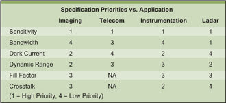
Figure 1. Reversing the trend of a few years ago, orders for linear and 2-D InGaAs imaging arrays are outpacing those for single-element InGaAs telecom detectors.
InGaAs cameras dovetail well with other imaging equipment. They provide analog video to standard TV or any commercial frame grabber card, and they can deliver simultaneous analog and digital outputs. Advanced military cameras transmit information so easily that command and control staff can see what a soldier in the field sees, as he sees it.
These imagers also can visualize eye-safe lasers and expand night-vision capabilities. There is five to seven times more energy from starlight and the glow of the night sky — even without moonlight — in the short-wave region than in any other spectral waveband.
Within the short-wave IR field, detectors based on InGaAs enable smaller and lighter uncooled imagers compared with those based on other material systems. Array sizes are growing as well. For every order placed for a single-element telecom detector today, there are three or four for the ever-larger linear or 2-D arrays for imaging. That’s just the reverse of five years ago. In fact, many current InGaAs telecom detectors are imaging devices because they combine many elements into arrays.
Interest in InGaAs short-wave IR technology has grown so quickly, especially for imaging, that it is outrunning its knowledge base for imaging system designers. As a result, many OEMs are forced to start their designs for vision systems using outdated, telecom-based, single-element specifications and design approaches because they can’t find anything better. In fact, more than half of the fabrication requests for custom InGaAs arrays seem to be built around these obsolete systems.
Three recent case studies illustrate why an OEM should work with a foundry that can provide design assistance based on the widest possible knowledge base. In all three, modifications from preliminary designs produced better performance, higher yields and lower costs.
High-speed imager
In the first case, a defense subcontractor was looking for small quantities of a 20,000-pixel InGaAs short-wave IR focal plane array for imaging equipment running at 1 billion cycles per second. The project plan revealed no details about the application, except that the illumination source would be a laser designator. The subcontractor wanted to optimize bandwidth and crosstalk suppression versus fill factor and to achieve high sensitivity and dynamic range.
The customer’s initial request was an array with pixels on a 100-μm pitch, bandwidth of 1 GHz, crosstalk of 0 dB, dark current of 1 pA and a fill factor of 100 percent. In fact, the sensitivity, fill factor and crosstalk specifications had been lifted directly from literature on a single-element telecom detector. The customer also had determined the location of the cathode connections and the general electronic scheme of the readout integrated circuit (not a particularly low-noise circuit) that was to mate with the detector.
Trade-offs between fill factor and crosstalk are inevitable: Minimizing crosstalk requires space between the pixels, which reduces fill factor. But an array made to the customer’s original specifications for bandwidth and sensitivity would have produced crosstalk of better than 50 percent. The pixel location of more than half of all the incoming photons would not be precisely known.
The customer was disappointed at first, but decided that low crosstalk was the more important of the two specifications and asked for suggestions for a revised design.
Starting with the specifications on the customer’s readout circuit, we derived a structural design for the detector array, eliminating unnecessary ones that could add cost or impair performance. Laser designators produce a lot of light, so the sensitivity specification was irrelevant. The readout circuit was not designed for low noise, so we could eliminate the dark current limitation on the detector. A detector need not be quieter than its mating readout circuit. This left speed, crosstalk and bandwidth as the truly relevant specifications.
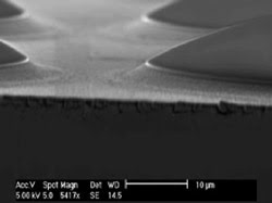
Figure 2. Microlenses helped regain fill factor and increase device bandwidth on a device whose pixel size had to shrink to meet crosstalk specs.
To achieve high speed, we recommended a low-capacitance structure with small pixels. To regain fill factor lost by decreasing the pixel size and to maintain bandwidth, we recommended etching microlenses into the optical plane of the array (Figure 2). The lenses would focus light onto the center of the active pixel. High-speed pixel design was cost-neutral, but the microlenses added approximately 15 percent to unit cost. Nevertheless, the changes made the difference between an array that works and one that would not.
The final deliverable consisted of our InGaAs detector, hybridized to the customer’s readout circuit to create a focal plane array assembly and wire-bonded to our custom ceramic submount. The submount mated noiselessly to a Kovar DIP package. Thermoelectric cooling was added to stabilize temperature, and the package was hermetically sealed in dry nitrogen with an antireflection-coated window to optimize optical performance of the high-bandwidth laser designator.
The design worked — the original would not have — and produced five times higher yields than the original array, saving 80 percent compared with the original cost estimates.
One can take from this case study the lesson that telecom specifications for single-element InGaAs detectors do not necessarily transfer to 2-D array imaging applications. Also, one should avoid overspecifying. Know which specifications are key, and back off the others.
 Another customer inquired about a detector mount for a 16-channel optical monitoring device for commercial telecom use, imposing very stringent demands for crosstalk (–40 dB), bandwidth (2.5 GHz) and yield (100 percent pixel operability). Additional key requirements included a quantum efficiency of 80 percent and a dark current limitation of 100 pA. The customer also provided samples of the mating optical interface: a fiber optic ribbon.
Unlike in the first case, this customer understood the application and design issues very well. The crosstalk limitation presented no challenge because there was no opposing fill-factor requirement. We could allow as much dead space between pixels as we felt necessary to limit the crosstalk because the pitch was greater than 200 μm.
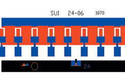
Figure 3. A customer who needed a detector mount for an optical monitoring device designed guards around each pixel to reduce crosstalk. As manufacturing ramped up, yields dropped because the guard design was vulnerable electrostatic discharge.
The customer’s design included two features intended to improve performance: guards around each pixel to reduce crosstalk (Figure 3) and a very compact front-illuminated detector layout. This design worked well for small quantities, but it produced low yields as production ramped up because the guard design was vulnerable to electrostatic discharge. Even minor charges triggered pixel dropouts in the arrays — unacceptable in light of the 100 percent pixel operability specification.
A change in the guarding scheme preserved the crosstalk performance level while eliminating sensitivity to electrostatic discharge (Figure 4). A modification in the mount made the customer’s final assembly more forgiving. Finally, refining the layout to bring in the optical and electrical interfaces at right angles saved more real estate while preserving the original capacitance and inductance limits.
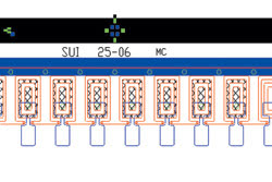
Figure 4. Redesigning the guarding scheme restored high-volume yields without affecting crosstalk performance.
These modifications resulted in the mass production of 64-pixel arrays in the same envelope and with the same yields as the 16-pixel arrays that were originally requested. The customer modified the device to capitalize on the change. The result was an 80 percent yield for the 64-pixel focal plane array mount, compared with a 50 percent yield for the original 16-pixel mount, reducing costs enormously. The 64-pixel detector also was both more forgiving in assembly and more powerful in performance.
This case teaches that, for high-volume devices, one should be ready to modify a prototype for manufacturability.
Scientific instrumentation
The third customer needed a focal plane array for an emission spectrometer used to troubleshoot CMOS devices. The instrument goes into a machine vision system for critical process control feedback in the fabrication of silicon chips. The detector was to be a low-speed, low-bandwidth device that operated at cryogenic temperatures, then cycled to room temperature when the unit was turned off.
The imaging system required a 320 × 256-detector array on a 25-μm pitch, with the ability to measure wavelength, intensity and position of light emitted from defects within a CMOS chip during testing. If one of these instruments were to go down, an entire chip line might stop cold; if it could not be delivered on time, some new CMOS line might have a start-up delay.
The instruments were to be low-volume but very high end, with extremely critical specifications for both performance and reliability. For the spectrometer to accurately measure both wavelength and intensity, every detector’s electrical response had to be absolutely linear with photonic intensity. And each pixel in the array had to respond exactly like its neighbor.
Other specifications for the detector included a dark current of less than 100 fA at room temperature and a pixel-to-pixel uniformity and response linearity of within 5 percent. The reliability requirement called for no separation of readout electronics over 100 thermal cycles between room and cryogenic temperatures. As mentioned, speed and bandwidth specifications were unremarkable.
Nonuniform material
A generalist foundry had been unable to meet either the dark current and uniformity standards or the delivery schedule. We found that, although the design was good, telecom-grade epitaxial material was not uniform enough to produce such a large array with such tight specifications (Figure 5). Furthermore, fabricating the devices on 2-in. wafers could not produce the required yields.
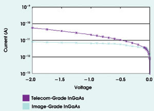
Figure 5. No foundry can make high-performance InGaAs detectors using low-grade materials. Moving from telecom-grade to image-grade epitaxial material enabled the production of large focal plane arrays to the desired tight specifications.
Using a new, proprietary epitaxial process that intrinsically produces detectors with low dark current, we were able to supply the customer’s requirements for performance within 3 percent response uniformity and to do so according to schedule. Also, by using 3-in. wafers, we increased the yield and saved money for the customer.
One can take three lessons from this example. First, be sure that the basic materials a foundry uses are adequate for your application. No foundry can make high-performance InGaAs detectors using low-grade substrates. Second, size matters in InGaAs wafers. The use of 3- or 4-in. wafers means bigger yields and lower unit costs than 2-in. wafers. Third, the InGaAs specialist may have proprietary technology that is years ahead of the generalist’s.
Meet the author
Michael J. Lange is director of fabrication technology at Sensors Unlimited Inc. in Princeton, N.J.; e-mail: [email protected].
Evaluating InGaAs Foundries
When looking for a foundry for an InGaAs detector application, consider the following:
• What is its installed base in custom InGaAs detectors for your application? Just as design principles from telecom do not necessarily transfer well to imaging or instrumentation, neither do fabrication capabilities.
• What size wafers does it use? The bigger the wafer, the higher the yield per wafer and the lower the cost, especially for large-area devices.
• What design assistance does it provide in InGaAs detector design? What is its experience base in design assistance for the application?
• What share of its foundry business is in InGaAs devices? InGaAs specialists can be several years ahead of generalist chip foundries in InGaAs technologies.
• How integrated is it? Can it provide epitaxial growth and readout circuit design as well as InGaAs device design, wafer fabrication, flip-chip hybridization, packaging and testing? Which processes does the foundry perform in-house, and which ones does it send out?