A simple solution-based electrical doping technique could help reduce the cost of polymer solar cells and organic electronic devices, and help move organic photovoltaics into a new generation of wearable devices.
Researchers at the Georgia Institute of Technology (Georgia Tech), the University of California at Santa Barbara, Kyushu University in Japan, and the Eindhoven University of Technology in the Netherlands developed the technique that provides a new way of inducing p-type electrical doping in organic semiconductor films. Their process involves briefly immersing the films in a solution at room temperature; this could replace more complex techniques that requires vacuum processing.

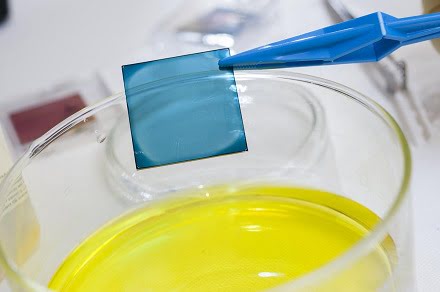
Graduate student Vladimir Kolesov holding an electrically-doped polymer film. Courtesy of Christopher Moore, Georgia Tech.
Bernard Kippelen, director of Georgia Tech's Center for Organic Photonics and Electronics, said "Our hope is that this will be a game-changer for organic photovoltaics by further simplifying the process for fabricating [a] polymer-based solar cell.”
Kippelen and his colleagues believe this new technique could impact other device platforms in areas such as organic printed electronics, sensors, photodetectors and LEDs.
The technique consists of immersing thin films of organic semiconductors and their blends in polyoxometalate (PMA and PTA) solutions in nitromethane for a few minutes. The diffusion of the dopant molecules into the films during immersion leads to efficient p-type electrical doping over a limited depth of 10 to 20 nm from the surface of the film. The p-doped regions show increased electrical conductivity and high work function, reduced solubility in the processing solvent, and improved photo-oxidation stability in air.
For the first time, single-layer polymer solar cells were demonstrated by combining this new method with spontaneous vertical phase separation of amine-containing polymers that leads to efficient electron collection at the opposing electrode.

Close-up of a polymer film on a glass substrate before immersion in a polyoxometalte solution to electrically dope the film over a limited depth. Courtesy of Christopher Moore, Georgia Tech.
Senior research scientist Canek Fuentes-Hernandez said the geometry of these new devices is unique, as the functions of hole and electron collection are actually built into the light-absorbing active layer, resulting in the simplest single-layer geometry with few interfaces.
"The realization of single-layer photovoltaics with our approach enables both electrodes in the device to be made out of low-cost conductive materials," said Fuentes-Hernandez. "This offers a dramatic simplification of a device geometry, and it improves the photo-oxidation stability of the donor polymer.”
Ph.D. Student Felipe Larrain hopes the new technique will allow fabrication of solar cells in areas that lack capital-intensive manufacturing capabilities.

Close-up of polymer films used in polymeric solar cells doped by
the new solution-based electrical doping technique. Courtesy of
Christopher Moore, Georgia Tech.
"Our goal is to further simplify the fabrication of organic solar cells to the point at which every material required to fabricate them may be included in a single kit that is offered to the public," Larrain said. "The solar cell product may be different if you are able to provide people with a solution that would allow them to make their own solar cells. It could one day enable people to power themselves and be independent off the grid.
The research done between these universities is different from others in that they are processing the films at room temperature.
"Being able to process solar cells entirely at room temperature using this simple solution-based technique could pave the way for a scalable and vacuum-free method of device fabrication, while significantly reducing the time and cost associated with it," said Vladimir Kolesov, a Ph.D. researcher.
Lifetime and cost analysis studies are still needed to assess the full impact of these innovations.
The research was sponsored by the Office of Naval Research and appeared in the journal Nature Materials (doi:10.1038/nmat4818).