Solar Cells, Array Films Constructed from Nanotubes
Michael A. Greenwood
Thin-film solar cells have been fabricated from double-walled carbon nanotubes, a material that is relatively untapped in photovoltaic designs but that offers high photoconductivity, mobility and stability.
Researchers from Tsinghua University in Beijing and from the University of Hawaii at Manoa in Honolulu recently demonstrated that macrosize bundles of the double-walled nanotubes generate a photocurrent, suggesting that the material is suitable for solar cells. Such nanotubes rarely have been used to fabricate organic solar cells.

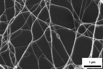
Figure 1. A scanning electron microscope images the porous network structure of double-walled carbon nanotubes. The tubes formed numerous heterojunctions on the silicon substrate.
The investigators created the cells by chemical vapor deposition. As part of the technique, the nanotubes were suspended in distilled water, where they expanded into an ultrathin film on the surface. The researchers transferred the nanotube film to an n-type bulk crystalline silicon substrate and allowed it to dry and adhere to the surface. A layer of titanium, palladium and silver was sputtered onto the substrate’s other side for the bottom electrode.
Lead researchers Jinquan Wei and Dehai Wu of Tsinghua said that the nanotubes created a porous network structure (Figure 1) and that numerous heterojunctions with the substrate were formed. The nanotubes occupied about 25 percent of the film area and had outer diameters of between 2 and 2.5 nm. Individual nanotubes were usually arranged in bundles ranging in size from 20 to 50 nm. The thickness of the film was fairly uniform at ∼50 nm, but could be adjusted by adding multiple layers.
To test the capabilities of the cells, the team connected an array of six to a red LED. The solar cells had a total working area of 3 cm2 and were irradiated by room light. The solar array powered the LED for more than 100 h without any obvious degradation. The nanotube cells achieved a power conversion efficiency of only ∼1 percent, but the researchers said that this could be enhanced by modifying the density and thickness of the nanotubes on the substrate and by upgrading the quality of the nanotubes themselves. Efficiencies of 5 percent, and even approaching 10 percent, could be attainable within three years, they said.
During experiments, cell thicknesses were adjusted from a low of 35 nm to a high of 250 nm by adding up to five layers of the nanotubes. The team found that, above four layers, at about 200 nm in thickness, the nanotubes became suspended and could not form junctions on the silicon. A thickness of 100 to 150 nm appears to be optimal, the researchers said.
Array films
In separate research with light-harvesting nanotubes, scientists at Pennsylvania State University in University Park have created vertically oriented nanotube array films fabricated from alloys of titanium and iron.
The films demonstrate properties useful for solar spectrum water photoelectrolysis, where water molecules are split to harvest the hydrogen for energy. Pure hydrogen is rare in nature.
The nanotube film was engineered to include the 2.2-eV bandgap of iron along with the exceptional charge-transfer properties and photochemical stability of titanium, said lead researcher Craig A. Grimes. The combined elements offer enhanced visible spectrum — from 380 to 650 nm — photoelectrochemical properties.
Researchers created the film by depositing titanium and iron metal films onto fluorine-doped tin-oxide-coated glass substrates by simultaneous co-sputtering. Films with varying iron content were fabricated.
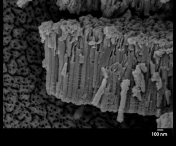
The investigators found that films with higher iron levels — approaching 100 percent — had diminished photoelectrochemical properties, so they used films with iron content ranging from 3.5 to 69 percent. The films were anodized at a constant voltage of 30 V in a solvent composed of ethylene glycol and ammonium fluoride. The amorphous samples were annealed in oxygen at 500 °C, resulting in nanotubes composed of a mixed titanium-iron-oxygen oxide (Figure 2).

Figure 2. A field emission scanning electron microscope image shows titanium-iron-oxygen nanotube arrays used for visible light water photoelectrolysis.
During tests, the nanotube array films achieved a peak photocurrent of 2 mA/cm2. A sustained, time-energy normalized hydrogen evolution rate by water splitting of 7.1 ml/W•h also was achieved.
The researchers reported that the thickness of the nanotube walls remains a problem. If the size can be reduced, photocurrents as high as 20 mA/cm2 likely could be achieved. The nanotubes used in the experiments had a wall thickness of 22 nm. The thickness ideally must be 4 or 5 nm. They are looking at ways to reduce the wall size.
Nano Letters, August 2007, pp. 2317-2321, 2356-2364.
Published: September 2007