Gustavo Asencios, Hamamatsu Corp.
A current trend in the optical detector industry involves the need for photodetectors that feature added capabilities. It used to be the case that the most efficient setup was a simple photodiode mounted on a PC board and a discrete amplifier, but times have changed. A new breed of photodetector is slowly making its way into applications once dominated by discrete components. There are many names for this type of device, which combines a photodetector and an integrated circuit. In this article, we will refer to such a device as a “photo IC.”
The benefits of an integrated solution are numerous, including in performance, price and size. When the signal-processing chip and the photodiode are integrated in a single package, the resulting product has better resistance to electromagnetic noise than its discrete counterparts and does not require complex analog design. Integration also enables lower pricing when produced in quantity. And a photo IC has a smaller footprint than a photodiode and discrete components for signal processing.
The variety of photo ICs available is dizzying, from simple phototransistors and transistor-based current amplifiers to light-to-frequency and charge amplifiers. The most common may be the pickup assembly in a CD-RW, an example of a custom design for a specific requirement, combining proprietary photodiode, circuitry and packaging.

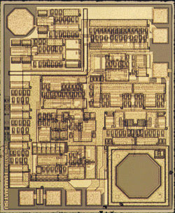
Figure 1. An image of a monolithic photo IC shows the photodiode and circuit on one chip.
Two types of photo ICs are available: monolithic and hybrid. In the former, the photodiode and signal processor are embedded in the same chip (Figure 1). This reduces stray capacitance in the system and makes it very strong against external noise because there are no wire bonds connecting the photodiode and circuitry. The drawback of the monolithic approach is that the wafer process is not ideal for the performance of the photodiode.
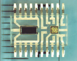
In a hybrid photo IC, the photodiode and signal circuitry are processed separately in different chips, and they are subsequently wire-bonded and packaged together (Figure 2). This maximizes their performance because the wafer processes can be optimized for each component. The hybrid design uses wire bonds between the detector and circuit, however, so it is not as strong as the monolithic design against external noise, and it is typically slightly larger.

Figure 2. The hybrid photo IC features the photodiode and circuit on separate chips, connected by wire bonds.
This drive toward integration has led to the use of CMOS, rather than bipolar, technology in the design of signal-processing circuits. Although bipolar technology continues to be a good choice for some applications, it may not offer the ability to design complex logic and charge-amplifier circuitry. CMOS also has an edge in material management, which affects the cost and delivery time of the finished product.
The bipolar process requires that wafer material be made with impurity diffusion, epitaxial and buried layers that can be used only for a specific product. In contrast, the CMOS process requires only a common wafer, which can be used for any CMOS product. The CMOS wafer, as a result, is cheaper and readily available, and the cost savings trickle down to the photo IC.
An example of a novel photo IC is the CMOS charge amplifier, wherein a photodiode is combined with the amplifier in a hybrid or monolithic structure so as to detect low-light-level signals. A CMOS charge amplifier is a lower-cost alternative to low-noise transimpedance amplifiers, and it has applications in fluorescence detection for medical and analytical markets.
The CMOS charge amplifier setup profits from an advantage of photo ICs: strong isolation from external noise sources. This is important in a low-light-level application because the photodiode’s signal output is very low. In comparison, an external transimpedance amplifier would require large feedback resistance — on the order of a gigaohm — and would face the challenge of the greater number of sources of noise in such a design with discrete components. The CMOS charge amplifier, with a built-in amplifier along with the photodiode, also allows less-strict design in the PC board, lessening the cost and time involved in design.
Besides the performance and cost advantages the photo IC carries, compactness is increasingly becoming one of the most sought-after features. A smaller footprint, available in a diverse range of packaging, is needed in a world where devices in the medical, industrial and consumer markets are becoming smaller and smaller. Miniaturization using CMOS technology also provides for lower power consumption, allowing longer battery life in many applications compared with bipolar and discrete designs. This adds to the many features welcomed by design engineers.
The growth in this field will be driven by the growth of its associated applications, such as media-oriented systems transport for automotive information systems, polymerase chain reaction equipment for biological threat identification in security applications and point-of-care cardiac enzyme monitors. These technologies are on the verge of becoming commonplace, and the use of photo ICs will help them do so.
Meet the author
Gustavo Asencios is marketing engineer at Hamamatsu Corp. in Bridgewater, N.J.; e-mail: [email protected].