For precision machining applications, picosecond pulses have advantages over nanosecond and femtosecond pulses.
Dr. Thomas Herrmann and Bernhard Klimt, Lumera Laser GmbH, and Dipl. Ing. Frank Siegel, Laser Zentrum Hannover eV
Nanosecond pulses from Q-switched, solid-state lasers have long been used in a variety of machining applications. More precise micromachining can be accomplished with the UV pulses from excimer lasers and with femtosecond pulses from ultrafast solid-state lasers, albeit it at a higher cost. Recent experiments have shown that picosecond pulses from diode-pumped solid-state lasers are capable of precise micromachining at surprisingly lower cost than the femtosecond alternatives.
Most industrial laser machining processes rely on the nanosecond pulses from Q-switched lasers such as Nd:YAG, which are sometimes shifted to shorter wavelengths with nonlinear optics. But nanosecond pulses, which ablate material by heating it, have definite limitations. They cannot achieve high-precision cutting, drilling or structuring on a micron scale because of thermal influences that cause microcracking, burr formation or resolidified debris. Although nanosecond laser systems are well-established, reliable and cost-effective, they cannot meet many of the demands for high-precision industrial processes.
Excimer lasers are often used for high-quality marking and machining of many materials. Their high-energy UV photons can break chemical bonds without significantly heating the material. But these lasers and the imaging optics they require are very expensive.
As with excimer lasers, femtosecond lasers can overcome the deleterious thermal effects of their nanosecond counterparts. In contrast to nanosecond laser processing, where the material is heated to the melting point, the material exposed to femtosecond pulses bursts immediately into plasma.
This so-called “cold” ablation process leads to precise structures limited only by the optical system that is used. But despite their advantages in precision, and their great flexibility (wavelength and pulse duration are principally adjustable), amplified femtosecond laser systems are of limited use in industrial applications because they are complicated, less reliable and often not cost-effective. Their repetition rate is restricted to a few kilohertz and their average power, to a few watts.
Heat-affected zone
Experimental investigations of drilling metals have shown that even femtosecond pulses can sometimes cause deleterious thermal effects. The metal vapor plume develops on a timescale many orders of magnitude longer than the ultrashort laser pulses. Therefore, even if the ablation process itself is “cold,” the expansion of the hot plasma transfers some heat to the surrounding material that can cause a heat-affected zone in the workpiece.
But reducing the pulse duration from a nanosecond generally will increase the precision of many machining applications. Experiments and theoretical considerations indicate that laser pulses with a duration of about 10 ps are ideal for many of them.1 Of course, obtaining optimum results depends on many parameters, such as pulse energy, focus, repetition rate, speed of focus movement and loop repeats, polarization control, etc. But we believe that reducing the pulse duration to values shorter than 10 ps does not significantly increase machining quality. Instead, shorter pulses may cause strong deformation of the laser beam near focus because of nonlinear processes in the air in front of the target surface. Considerable energy can be lost or deflected from the target area so that precision is compromised.
Picosecond lasers, in many cases, are capable of precision as great as excimer and femtosecond lasers. They are much less complex and more reliable. Their usage is less expensive (cost per part machined) than that of those systems. They have a much lower cost of ownership than excimer lasers. Compared with femtosecond laser systems, they have fewer optical components, they don’t need sophisticated chirped-pulse amplifiers and their repetition frequencies can be as high as 100 kHz (compared with several kilohertz).
Thus, picosecond lasers, such as the Staccato, produced by Lumera Laser GmbH in Kaiserslautern, Germany, promise to combine the best of both technologies. They provide the repetition rate and, potentially, the reliability of nanosecond lasers, together with the fundamentally nonthermal machining capabilities of femtosecond lasers. Their high repetition rate maximizes throughput and cuts the cost per part. Finally, because they have high peak powers, their outputs can be efficiently converted to shorter wavelengths with nonlinear optics.
The Staccato offers sufficient pulse energy for precise micromachining at repetition rates of up to 100 kHz and this can drastically reduce processing time and cost while maintaining high machining quality: It can cut 100-μm steel sheets — at 0.4 mm/s using a 2-W (100 kHz, 20 μJ) beam. This is more than 10 times faster than is possible with a beam of femtosecond pulses in the same application. A machining system applying the laser’s full 10 W (possibly in parallel beams) could increase the throughput again by a factor of five.
A diode-pumped Nd:YVO4 laser, it delivers pulse energies up to 100 μJ at 100 kHz in pulses shorter than15 ps. The laser is based on an all-solid-state picosecond oscillator that generates more than 2 W of average power at a repetition rate of 50 MHz and a pulse energy of more than 40 nJ. Electro-optic modulators with ultrafast high-voltage switches select a single picosecond pulse at repetition rates of up to 100 kHz. The selected pulses are boosted to more than 100 μJ in a regenerative amplifier, maintaining very good beam quality. (M2 <1.5 is specified, and much better values are measured.) Focusing such high-energy pulses to 10-μm spot sizes creates peak power densities in the 10 TW/cm2 range, allowing virtually any material to be processed. The frequency conversion of pulses with such high power density is efficient; for instance, at 50 kHz, 100 μJ can be generated at 532 nm, 40 μJ at 355 nm or 20 μJ at 266 nm.
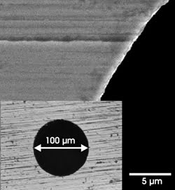
Hole drilling in stainless steel is one application suited to picosecond lasers. Techniques have been developed to meet industrial requirements for surface quality and speed. In helical drilling, the laser beam penetrates the workpiece on a helical path (Figure 1). The edge quality of the cut is excellent (see the scanning electron microscope picture in the background) compared with the results obtained from nanosecond laser machining.

Figure 1. This 100-μm-diameter hole was drilled in 100-μm-thick stainless steel with 30-μJ pulses from a picosecond laser.
Further improvement can be achieved by adapting the polarization of the laser light during the drilling process with regard to the cutting direction, because ripple formation on the surface of the hole wall and irregular hole shapes result from random polarization with regard to the wall. Special trepanning optics allow the E-vector to remain perpendicular to the wall.
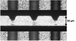
Another application that demonstrates the precision of picosecond-laser machining is material surfaces structuring (Figure 2). The image shows the laser’s accuracy with no burr formation or recast layer visible. Processing near the ablation threshold removes the material with minimal debris and heat-affected zone. This makes picosecond lasers attractive for applications where surface structuring or material removal in the micron range is required.

Figure 2. The grooves in 50-μm-thick stainless steel were scribed near the ablation threshold with minimal heat-affected zone. The overlay is a longitudinal view of the grooves.
The removal of thin indium tin oxide (ITO) layers is a promising application of picosecond systems. ITO layers are used to make transparent conductive coatings for panel contacts, liquid crystal display electrodes or electrochromic displays. Typically, ITO layers are only a few hundred nanometers thick, so they can be removed with low energy densities. Experimental investigations have shown the suitability of a picosecond laser system with high repetition rates to efficiently ablate the ITO layer without damaging the underlying materials. It is possible to cut ITO layers with structural features of 10 µm and less on a computer-controlled path with speeds of about 250 mm/s.
Six-axis positioner
Laser Zentrum Hannover eV scientists used a 532-nm picosecond laser in combination with a high-precision, six-axis positioning system to perform micromachining applications on metals and silicon wafers. The setup of the three linear and three rotary axes within the portal system allows the laser beam to be positioned on complex, three-dimensional workpieces with accuracy in the micron range. By using two linear movable deflection mirrors and one rotatable deflection mirror, the position of the laser focus and the direction of the beam can be adjusted. The design of the optical path allows a high degree of freedom with minor limitation regarding the angle of irradiation, which is an essential requirement for such fundamental micromachining investigations.2
This micromachining system also was used to structure metals and other industrially relevant materials (Figure 3). Here, a tapered hole and the resulting cone were cut out of a 1-mm-thick chrome-nickel alloy. The structure shows the high quality and high precision that picosecond laser systems provide by avoiding thermal effects. Such drilled-hole geometries are used as micronozzles along the outer wall of pipes for cleaning and coating devices.

Figure 3. Two of the applications for the picosecond laser/positioning system combination are, top and middle, drilling (CrNi) and, bottom, cutting (Si).
Another industrial application is cutting silicon wafers. Here, the kerfs between the chips must be as small as possible to optimize the packing onto the wafer. Additionally, a high-quality cutting edge is required to avoid postprocessing. The use of picosecond laser pulses eliminates the formation of cracks near the cutting edges, and no cleaning or other postmachining processes are necessary. Because of silicon’s higher absorption in the UV, we expect that applying UV picosecond pulses will raise the cutting speed over that achieved with 532-nm radiation while preserving the good edge quality.
Teflon is widely used in electronics and medical applications. Its material properties prevent the machining of very small structural details, and it cannot be machined with the longer-wavelength excimer lasers because it has low absorptance at those wavelengths. Only 157-nm F2 lasers provide clean cuts without thermal damage, but such processing systems require an oxygen-free environment and expensive optics.
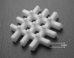
We recently demonstrated that picosecond lasers can machine Teflon nonthermally under normal atmospheric conditions (Figure 4). In cooperation with a German biotech company, this prototype of a support structure for a liquid filtering system was machined out of a Teflon block. Because the liquids that the system handles are often corrosive, the use of an inert material like Teflon was essential.
Cutting diamond is another promising application of picosecond lasers. The high repetition rate that is possible with picosecond pulses enables efficient cutting of diamond without causing thermal damage to the bulk material.

Figure 4. This Teflon support structure designed for a liquid filtering system was machined out of a Teflon block. The material removal rate was 0.2 mm3/s using picosecond pulses at 50 kHz.
For micromachining and structuring very thin films or coatings, the very high repetition rates of quasi-CW picosecond lasers are advantageous. It is possible to structure 5-μm layers of SiN on Si at 5 m/s under computer control. The laser oscillator operates at 160 MHz, providing 16 W of average power, a pulse duration of 10 ps and a nearly diffraction-limited output.
Other applications of the quasi-CW lasers include direct writing and imaging, digital printing, fluorescence imaging, spectroscopy, laser pumping, materials research and local curing of photo resins.
In summary, picosecond lasers have proved to micromachine industrially relevant material with the highest quality possible and have the potential to reduce the cost per part by an order of magnitude because of their high repetition rates. These factors and their reliability open the door for new industrial laser micromachining applications.
References
1. F. Dausinger, H. Hügel and V. Konov (2002). Micro-machining with ultrashort laser pulses: From basic understanding to technical applications. Konferenz ALT ’02.
2. H.K. Tönshoff, A. Ostendorf, C. Kulik and F. Siegel (2003). Finishing of cutting tools using selective material ablation. Proc. of First International CIRP Seminar on Micro and Nano Technology.
Meet the authors
Thomas Herrmann heads the applications lab at Lumera Laser GmbH in Kaiserslautern, Germany.
Bernhard Klimt is responsible for marketing and sales at Lumera Laser.
Frank Siegel is a project manager at Laser Zentrum Hannover eV.