Demands from advanced applications are sparking new techniques.
Dr. Alexandre Pauchard and Dr. Alexis Rochas, id Quantique
Standard PIN and linear-mode avalanche photodiodes are the devices of choice for most light-detection applications. However, at ultralow-light levels, these detectors fall short because the noise of the readout electronics becomes greater than the photodiode signal. In a wide range of research and commercial applications — such as fluorescence and luminescence detection, DNA sequencing, fluorescence correlation spectroscopy, decay time measurements, flow cytometry, noncontact profilometry, particle sizing and astronomy, as well as military and commercial lidar applications — the detection of just a few photons is essential.
Photomultiplier tubes and Geiger-mode avalanche photodiodes — commonly called photon counters — were developed specifically to excel at ultralow-light levels. Although these devices can detect single photons, it is a mistake to call them photon counters because they cannot resolve photon quantity. Instead, they are trigger devices: They indicate if one or more photons have hit the detector’s active area but usually cannot distinguish between the arrivals of one or more photons.
Light detection evolves
Photomultiplier tubes have been produced industrially since the 1950s. Major suppliers, such as Hamamatsu Photonics KK of Japan and Burle Electro-Optics Inc. of Sturbridge, Mass., have introduced refinements over the years.
Solid-state avalanche detectors, on the other hand, became available in the 1990s. PerkinElmer Optoelectronics of Fremont, Calif., in particular, was successful with its single-photon-counting module. The avalanche photodiode at the heart of the module is fabricated with a nonstandard custom silicon process that uses ultrapure, high-resistivity wafers. The active area diameter of the detector is about 160 μm. Thanks to a thick depletion layer, the photon-detection efficiency is high in the visible region. But for the same reason, the photon-timing resolution (also called timing jitter) is poor: about 350 ps full width half maximum. The fabrication technology is inherently complex, which means that the production yield of good devices is low and the cost, high.
There is no prospect for producing on-chip avalanche photodiode arrays using this technology: Only single-pixel elements are available. Furthermore, these detectors are damaged by strong illumination, and intrinsic high-power dissipation means that effective cooling is necessary.
Better timing, spatial resolution
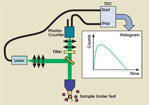
Over the past few years, the need for improved photon-counting detectors has increased dramatically, driven by progressively more demanding applications. Rugged counters with good timing resolution are desirable, for example, in time-correlated photon-counting techniques, which are used for single-molecule detection and advanced fluorescence lifetime measurements (Figure 1). Likewise, high-spatial-resolution photon counter arrays (one- and two-dimensional) are needed for high-throughput and mapping applications, and DNA sequencing using single-molecule-array technology has the potential to transform the economics of the process by allowing millions of individual DNA molecules to be rapidly sequenced in parallel.

Figure 1. This setup was used for time-correlated single-photon-counting measurements. TDC = time-to-digital converter.
Three-dimensional lidar imaging, which is of high importance for military and commercial markets, is another application requiring photon-counter arrays. On the military side, 3-D imaging facilitates the detection of masked or occluded targets; commercial applications include terrain mapping and obstacle avoidance for autonomous vehicles.
The CMOS generation
To overcome the limitations of photon counters, several academic research groups have worked on next-generation devices. The major breakthrough came from the use of CMOS for device fabrication — a technology widely used in the microelectronics industry. For example, a group of scientists at the Swiss Federal Institute of Technology in Lausanne used a standard commercial CMOS process to create an 8 × 4-pixel avalanche photodiode array and demonstrated an excellent timing resolution of 40 ps.
Using a CMOS process to fabricate photodetectors has several advantages: It becomes possible to fabricate large avalanche photodiode arrays, to significantly reduce timing jitter, thanks to the use of devices with narrower depletion regions, and to integrate the electronics and the photodiode on the same silicon chip to drastically reduce fabrication cost.
Alternatively, researchers at Politecnico di Milano in Italy have followed a hybrid approach, with the readout electronics fabricated in a CMOS process and the avalanche photodiode fabricated in a custom planar epitaxial process. And a group at the National Microelectronics Research Centre (now part of the Tyndall National Institute) at the University of Cork in Ireland has done similar work using a CMOS-compatible process for making avalanche photodiodes.
Photon counters based on the CMOS method are being commercialized. Id Quantique offers two products based on this technology: the id100, a compact single-element photon counter, and the id150, a one-dimensional 1 × 10 photon-counter array for high-through-put measurements. These compact modules do not require thermoelectric cooling, and even with the detector, biasing and readout electronics integrated within each pixel, the pitch is still only 50 μm (Figure 2).

Figure 2. A close-up view of the 1 × 10 avalanche photodiode array shows the detector, biasing and readout electronics integrated within each pixel.
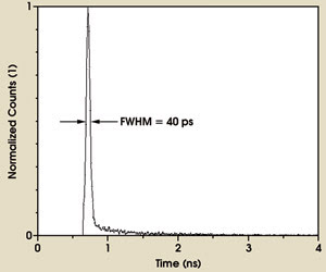
The Milan and Cork groups are also working toward the commercialization of their devices. Because these detectors have thinner active regions, their photon-detection probability in the blue region is better than that of the PerkinElmer module (20 percent vs. 8 percent at 400 nm), but the sensitivity in the red and NIR regions is smaller (20 percent vs. 70 percent at 700 nm). This is the price to pay for achieving a timing resolution of 40 ps (Figure 3).

Figure 3. The graph shows the measured timing resolution of the id100 and id150.
Another advantage of CMOS-based photon counters is that they consume one-tenth of the power of non-CMOS devices because of a low internal operating voltage (25 V) and the fact that no cooling is required. Furthermore, these detectors do not suffer from memory effects exhibited by photomultiplier tubes and, unlike single-photon-counting modules, are not damaged by ambient light. A current limitation of CMOS-based devices, however, is the smaller active area — typically smaller than 100 μm. Also, the dark count rate of devices with a larger active area is still too high.
Detection in the infrared
The detection of single photons in the IR range is more problematic. Although photomultiplier tubes with a spectral response extending to 1700 nm exist, their efficiency does not exceed a fraction of a percent. Superconducting materials have been tested, but their cooling requirements make them impractical for most applications. The InGaAs/InP avalanche photodiode — originally developed for optical communications applications — is the device of choice for photon counting in the IR range. A high dark count and after-pulse density, unfortunately, plague these detectors.
In applications where the arrival time of a photon on the detector is known with precision, such as quantum cryptography or optical time-domain reflectometry, it is possible to use the gated mode of operation. In this approach, the excess bias voltage across the avalanche photodiode is raised above the breakdown voltage when a photon is expected. This typically lasts only a few nanoseconds. The technique enables id Quantique’s id200 counting module to achieve a quantum detection efficiency of more than 10 percent at 1300 and 1550 nm.

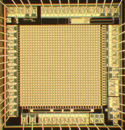
Figure 4. A 3-D image sensor has been developed at the Swiss Federal Institute of Technology. Courtesy of Edoardo Charbon.
The next step in the evolution of CMOS-based photon counters may be the development of large arrays for 2-D and 3-D imaging. A number of applications — including facial recognition, object monitoring, smart air-bag deployment systems and nonionizing medical tomography — require fast and precise depth-map evaluation and, hence, could benefit from these sensors.
TOF sensor
A 3-D image sensor based on the time-of-flight method has already been demonstrated by the Swiss group. It consists of a 32 × 32 avalanche photodiode array fabricated in a commercial CMOS process (Figure 4). After having already made contributions in fields from microelectronics to image sensors, CMOS technology may continue to revolutionize the way we count single photons.
Meet the authors
Alexandre Pauchard is vice president of engineering at id Quantique in Carouge, Switzerland; e-mail: [email protected].
Alexis Rochas is responsible for the development of the company’s single-photon detectors; e-mail: [email protected].
Have You Seen a Single Photon Lately?
We all know that photons are tiny. For one thing, a photon has no mass (the limit has been measured at below 10–51 g). A photon with a wavelength of 800 nm has an energy of only 2.5 × 10⁻¹⁹ J, or 1.55 eV.
Humans can see a huge range of intensities, from daylight levels of around 108 cd/m2 to night luminances of approximately 10–6 cd/m2. How many photons must arrive at the eye every second for our brain to consciously register a signal? About 600.
Though incredibly sensitive, the human eye is not perfect. Its efficiency is about 10 percent, meaning that only 60 of the initial 600 photons will reach the rods, the receptors on the retina at the back of the eye responsible for low-intensity vision. The rest of the signal is lost. It is reflected (3 percent) or absorbed by nonsensing parts (47 percent), or it falls between the rods (40 percent).