Ansheng Liu, Intel Corp., Santa Clara, Calif.
High-speed optical modulators are a key component for optical communications and for future optical interconnect applications. Today’s commercially available optical modulators at 10 Gb/s are based on electro-optic materials such as lithium niobate and III-V compound semiconductors. These devices have demonstrated modulation capability as high as 40 Gb/s. To achieve similar performance in silicon is challenging because crystalline silicon exhibits no linear electro-optic (Pockels) effect. Engineers are forced to rely on the free-carrier plasma dispersion effect, in which the refractive index is changed when free-carrier density is varied, to modulate light in silicon. To date, the fastest data transmission demonstrated in silicon has been ∼10 Gb/s.
At Intel Corp. in Santa Clara, Calif., and in Jerusalem, we have designed and fabricated a silicon optical modulator that can transmit data at 30 Gb/s — we believe a world record. We also believe that the concept is scalable to speeds of 40 Gb/s and beyond. The modulator still relies on the free-carrier effect, but its high speed is the result of a device design with a traveling-wave drive scheme. The work is detailed in the Jan. 22 issue of Optics Express.
The Intel modulator is based on a Mach-Zehnder interferometer with a reverse-biased p-n junction in each of the arms (Figure 1). When a reverse voltage is applied to the junction, free carriers — electrons and holes resulting from the n- and p-dopants — are pulled out of the junction, changing its refractive index via the free-carrier effect. The intensity of the light transmitted through the Mach-Zehnder interferometer is modulated by adjusting the phase difference between the interferometer’s two arms.
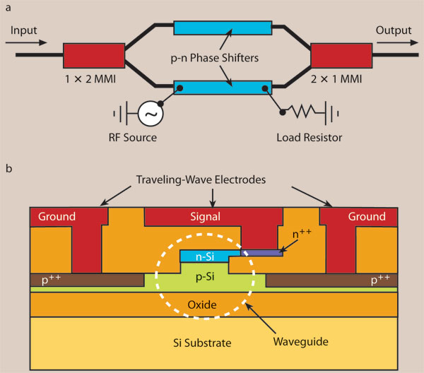
Figure 1. The Mach-Zehnder interferometer silicon modulator contains two reverse-biased p-n diode phase shifters (a). The splitters are multimode interference (MMI) couplers. The radio-frequency (RF) signal is coupled to the traveling-wave electrode from the optical input side, and termination load is added to the output side. The cross-sectional view in (b) shows a p-n junction waveguide phase shifter on silicon on insulator. The refractive index modulation is based on the depletion width variation in response to the reverse bias voltage caused by the free-carrier plasma dispersion effect in silicon. The coplanar waveguide electrode was designed to match the electrical and optical velocities. Images reprinted with permission of Optics Express.

This modulation can be very fast, because free carriers can be swept out of the junction with a time of approximately 7 ps. The modulator speed is thus limited by the parasitic effects, such as resistance capacitance time constant limit.
To minimize this limitation, we adopted a traveling-wave drive scheme, allowing electrical and optical signal copropagation along the waveguide. The traveling-wave electrode — which is based on a coplanar waveguide — was designed to match the velocity for both optical and electrical signals, while keeping the radio-frequency attenuation small.
To operate the traveling-wave modulator, the radio-frequency signal is fed into the transmission line using a commercially available driver from the optical input side, and the transmission line is terminated with an external resistor (Figure 1a).
After packaging the modulator on a printed circuit board, the researchers demonstrated that the modulator has a 3-dB bandwidth of ∼20 GHz and data transmission capability up to 30 Gb/s (Figure 2).
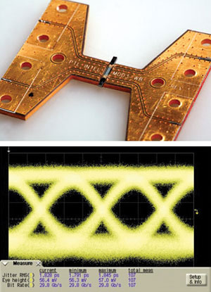
Figure 2. The silicon optical modulator is packaged on a printed circuit board (top). The Mach-Zehnder modulator that produced this eye diagram (bottom) has a pair of 1-mm-long phase shifters. One of the phase shifters is driven by a radio-frequency signal with a bit rate of 30 Gb/s.
The high-speed silicon modulator could find use in various future applications. For example, a highly integrated silicon photonic circuit may provide a cost-effective solution for the future optical interconnects within computers and other devices. With the demonstration of the 30 Gb/s silicon modulator and the electrically pumped hybrid silicon laser (Photonics Spectra, January, p. 54), it will become possible in the near future to create a single chip that can transmit data at a data rate of terabits per second.
Meet the author
Ansheng Liu is principal engineer at Intel Corp. in Santa Clara, Calif.