The performance of silicon photodiode integrated circuits is better than the material properties and device physics of silicon optoelectronic devices suggest.
Jürgen Leeb, A3PICs Electronics Development GmbH
The ever-increasing data rates of modern telecommunications networks demand low-cost optical interconnects between or within electronic systems to overcome the bottleneck of electrical interconnects. The interface between optical and electrical signals usually is an optical receiver that converts the light with a photosensitive device (photodiode) into a photocurrent and delivers electrical output signals that are appropriate for the following receiving unit.
In modern high-speed data transmission systems, such optical receivers have to meet a number of requirements concerning bandwidth, sensitivity, immunity to electromagnetic interference and reliability. From a more commercial point of view, low production costs — and, therefore, minimum chip size, simple assembling processes and the use of well-established semiconductor technologies — are important for the realization of competitive products in the consumer electronics sector.
Photodiode integrated circuits monolithically integrate the photosensitive device and the electrical circuitry that amplifies the photocurrent delivered by the photodiode, so that the output is suitable for subsequent signal processing. The integration of the photodetector and the amplifier in a single chip allows bond and solder connections to be eliminated, which improves the system’s performance over that of two-chip solutions that employ a separate photodiode and amplifier.
The improvement is multifaceted. Because of lower parasitic capacitance, it is possible to create receivers with a higher bandwidth that are well suited for systems with higher data rates. The shorter connection between the photodiode and amplifier increases the immunity of the receiver to electromagnetic interference. The elimination of the bond and solder connections means less fault liability, easier assembling processes and reduced chip area. And the weight of optoelectronics systems can be reduced, which is important in many applications, such as in the pickup units in optical storage systems.
Materials choice
When it comes to comparing semiconductor materials for integrated photodetectors, the most important parameter is the optical absorption coefficient, α. In general, a higher absorption coefficient leads to a higher photocurrent produced by a given incoming optical signal. It determines the penetration depth 1/α of light with intensity I0 in the semiconductor material according to the Beer-Lambert law:

where y is the coordinate perpendicular to the surface of the semiconductor.
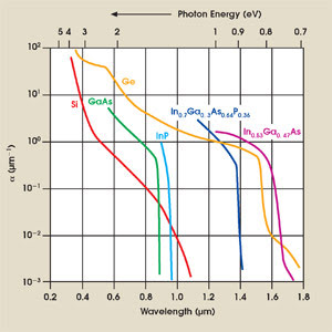
Figure 1. The optical absorption coefficient, α, determines thepenetration depth of light in a material and depends strongly on wavelength. In semiconductor materials for photodetectors, a higher absorption coefficient generally corresponds to a higher generated photocurrent for a given incoming optical signal.
The absorption coefficients of different materials depend strongly on the wavelength of the incident radiation (Figure 1). For wavelengths shorter than λc, which corresponds to the bandgap energy Eg (λc = hco/Eg, where h = Planck’s constant and co = speed of light in vacuum), the absorption coefficients increase rapidly according to the so-called fundamental absorption. From the figure, it follows that InGaAs and Ge cover the widest wavelength range — including the wavelengths around 1.3 and 1.54 μm, which are used for long-distance optical data transmission via optical fibers. The absorption coefficients of the direct-bandgap materials GaAs and InP are high at shorter wavelengths. These materials are used for detectors in short-distance optical interconnects via free space and for data links with inexpensive plastic optical fibers.
Generally, the direct bandgap materials show a steep increase in the optical absorption coefficient for λ<λc. Silicon, however, is an indirect-bandgap material, for which the optical absorption coefficient increases slowly for λ<λc. The absorption coefficient of silicon, therefore, is one to two orders of magnitude lower than that of the direct-bandgap semiconductors in this spectral range. The better optical properties and the larger electron mobility of GaAs compared with silicon, and the availability of very rapid electrical components, explain why GaAs-based photodiode integrated circuits traditionally are used for high-speed optical receivers.
It is a common belief that compound-semiconductor materials with a direct bandgap such as GaAs have large optical absorption coefficients and achieve a high quantum efficiency with a thin absorption region, leading to high-speed photodiodes. The benefits of GaAs, however, are at the expense of a lower production yield than can be obtained with silicon, which limits the number of transistors to about 105 per chip. A silicon chip can contain more than 108 transistors. Other drawbacks of GaAs are higher wafer and chip costs compared with solutions in well-established silicon technologies.
Silicon technology’s lower cost is advantageous in mass-produced applications such as optical storage and high-speed short-range optical interconnects. Another application for which inexpensive silicon photodiode integrated circuit technology is well suited is in the plastic fiber optical networks that are becoming widespread in the automotive industry.
Transient response
Because silicon has an indirect bandgap, its absorption coefficient is small, and light in the spectral range of interest, 600 to 850 nm, penetrates more deeply into it than into a compound semiconductor. Space-charge regions are thin because the substrate doping concentrations are larger than 1015/cm3 and because the voltage applied to the chip is typically 5 V or less. Therefore, the diffusion of charge carriers photogenerated below the space-charge region in the substrate or close to a PN junction slows down the transient response of the photodiode.
This can be avoided by employing a PIN photodiode structure: a photodiode with an undoped or low-doped intrinsic region sandwiched between the P- and N-type materials. The purpose of the intrinsic region is to extend the depletion region, preventing carrier diffusion. In a possible structure for an integrated PIN photodiode, the intrinsic region comprises an N– and a P– epitaxial layer, resulting in greater thickness, dI (Figure 2).
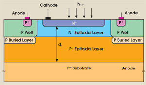
Figure 2. The cross section of a monolithically integrated silicon PIN photodiode illustrates the intrinsic region sandwiched between P- and N-type materials. The device structure extends the depletion region, thereby avoiding carrier diffusion.
But the adoption of a PIN structure is not without consequences. An important parameter in determining the speed of a photodiode is the drift velocity, vdrift, of photogenerated carriers in the semiconductor:

where E is the electric field, μ is the charge-carrier mobility, VPD is the photodiode supply voltage, and dI is the thickness of the absorption region. The thicker the absorption region of a photodiode, the smaller the electric field for a given applied voltage, and the smaller the electric field, the lower the drift velocity. Thus, the deeper absorption region of a silicon PIN photodiode, which is necessary to increase the quantum efficiency, directly diminishes its speed.
To speed up a PIN photodiode, one can increase the electric field with another, higher supply voltage. This boosts the drift velocity of the carriers, so long as the saturation velocity is not reached and the space-charge region is not widened.
GaAs vs. silicon
To compare GaAs and silicon photodiode integrated circuits, consider a monolithic integrated GaAs optoelectronic receiver with a large-area photodiode described by researchers at Fraunhofer Institut für Angewandte Festkörperphysik in Freiburg, Germany.1 For low-cost fiber interconnects, large photodiodes are advantageous because they can tolerate large misalignment between the multimode optical fiber and the photodiode.
In the researchers’ receiver, a metal-semiconductor-metal photodiode with a diameter of 300 μm, a capacitance of 1 pF and a responsivity of 0.22 A/W was monolithically integrated with a transimpedance amplifier, a high-gain amplifier and a limiting output buffer. They reported a sensitivity of –15.7 dBm and a bit error rate of 10–9 at 2.5 Gb/s. The total power consumption was about 500 mW, and the chip size was 3 × 1.5 mm (Figure 3a).
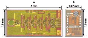
Figure 3. There is a dramatic difference in the chip size of a GaAs photodiode integrated circuit (a) and a device realized in silicon (b). Figure 3a courtesy of Fraunhofer Institut für Angewandte Festkörperphysik. PD 5 Photodiode. VUC 5 Voltage Up-Converter.
Now consider a 2.5-Gb/s silicon receiver with an integrated large-diameter PIN photodiode developed at Technische Universität Wien in Austria.2 In this silicon photodiode integrated circuit, a 300-μm PIN photodiode with a responsivity of 0.36 A/W at 660 nm and a capacitance of 1.14 pF at a reverse bias of 12 V was monolithically integrated with a transimpedance amplifier and a limiting postamplifier (Figure 3b). Even with the additional voltage up-converter, the silicon device was less than one-third the size of the GaAs photodiode integrated circuit. The measured sensitivity was –20.1 dBm in this receiver, with a bit error rate of 10–9 at 2.5 Gb/s (Figure 4).
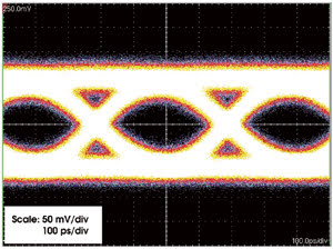
Figure 4. The silicon photodiode integrated circuit displayed a measured sensitivity of –20.1 dBm with a bit error rate of 10–9 at 2.5 Gb/s.
The sensitivity of the silicon photodiode integrated circuit was 4.4 dB better than that of the GaAs. In other words, the GaAs receiver needs 2.75 times the optical input power to achieve the same low bit error rate as the silicon device.
Another advantage of the silicon circuit involves the separate power supply for the photodiode. The Austrian university has demonstrated an on-chip, low-noise charge pump that acts as a voltage up-converter to generate the voltage required for the photodiode (Figure 5).3 This is a considerably less expensive solution than a separate 10-V power supply, as in the GaAs metal-semiconductor-metal photodiode.
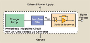
Figure 5. A low-noise charge pump generates the voltage required by the photodiode.
Another silicon photodiode integrated circuit with a diameter of 50 μm has displayed an even better sensitivity, –24.3 dBm at 660 nm, and a 3-Gb/s data rate, confirming that the on-chip charge pump does not disturb the optical receiver.
Promising developments
There continues to be progress in silicon photodiode integrated circuit technology. Receivers for plastic optical fibers have been fabricated, with photodiode diameters of 400 to 500 μm and sensitivities from –20 to –23 dBm at data rates of 250 to 300 Mb/s. Single-stage transimpedance amplifiers have been realized with a gain of 195 kΩ at a bandwidth of 380 MHz, allowing lower power consumption, lower offset voltage and smaller chip areas. Voltage up-converters for output currents up to 1 mA with an active chip area of less than 0.74 × 0.54 mm have been demonstrated.
Therefore, a maximum average optical input power of 2.78 mW is possible (with a photodiode responsivity of 0.36 A/W), resulting in a dynamic input power range of 24.5 dB (for the sensitivity of –20.1 dBm mentioned above). The possible peak optical input power is 2 or 3 dB higher.
Silicon photodiode integrated circuits are better than one would expect after a first comparison of the material properties and device physics of silicon and III-V semiconductor optoelectronic devices. They can easily cover data rates in most of today’s mass-market optical detector applications, such as the optical pickup heads in CD-ROM, DVD and Blu-Ray media storage solutions, and the plastic optical fiber receivers for fiber-in-the-home and for optical buses in automobiles.
Another potential application will be in the optical interconnects on electro-optical boards, via optical backplanes and free-space approaches, avoiding electrical interference and reflections in pure electrical systems.
Meet the author
Jürgen Leeb is managing director of A3PICs Electronics Development GmbH in Eichgraben, Austria; e-mail: [email protected].
References
1. M. Lang et al (Sept. 27, 2001). Complete monolithic integrated 2.5 Gbit/s optoelectronic receiver with large area MSM photodiode for 850 nm wavelength. ELECTRON LETT, pp. 1247-1249.
2. R. Swoboda and H. Zimmermann (April 15, 2004). 2.5 Gbit/s silicon receiver OEIC with large diameter photodiode. ELECTRON LETT, pp. 505-507.
3. R. Swoboda et al (2004). A 2.4 GHz-bandwidth OEIC with voltage-up-converter. Proc. 30th European Solid-State Circuits Conference, pp. 223-226.