BARRY SILVERSTEIN, META’S REALITY LABS
Industrial manufacturing has long favored silicon carbide (SiC) for its utility as a cutting material, exhibiting exceptional hardness that resembles diamond at roughly half the cost. Other desirable qualities, including SiC’s mechanical strength, thermal conductivity, and low density, have steered the material into the field of optics to be used as a thin, lightweight, and stable coated optical mirror substrate for space applications.
More recently, SiC’s distinct electrical and mechanical properties have been applied to gain efficiencies and reduce costs for power electronics. When manufactured as a single crystal (with sufficient purity and doping), SiC delivers a wide bandgap, high critical electric fields, and thermal conductivity that enable commercial power electronics to operate at high voltages and temperatures without breakdown.
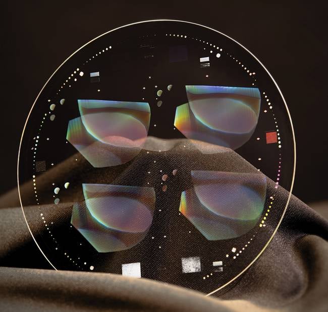
AR devices promise to expedite the adoption of silicon carbide (SiC) and unlock possibilities for human-computer interaction — including wide FOV wearable displays. Courtesy of Meta.
In turn, this enables lighter, smaller, thermally resilient, and more efficient components for electrical applications in transmission and inversion/conversion for the rapidly growing electric vehicle and alternative energy sectors. In data center usage alone, such efficiency gains are expected to drop cooling costs by roughly 25% to 40% per system. And in alternative energy switching, it is estimated that using SiC can enable system efficiencies as high as 98% from the kilowatt to megawatt power ranges1.
Further, as grown SiC crystals are increasingly purified and manufactured with suitable defects, fabricators have realized single crystal wafers with very high resistance in support of high-speed microwave radio frequency switching. High electron mobility transistor devices are already used to enable 5G and next-generation communication systems.
At the same time, bottlenecks hinder the broad and widespread adoption of SiC. The material is hard to produce compared with silicon due to the high temperature physical vapor transport growth method. This technique involves heating precursor SiC powder to temperatures between 2300 and 2500 °C inside a graphite crucible. The individual steps involved in this process are prone to yielding unwanted material defects that may destroy necessary electronics properties. In situ monitoring of the process is challenged by the high temperatures. Subsequent processing steps of creating wafers and devices are more time-consuming and costly as a result of the robust mechanical properties.
Despite this significant limitation, however, manufacturers around the world broadly appreciate that SiC is a critical material supporting the shift toward a more electrically centered power infrastructure and an increased need for high-speed electronics with greater bandwidths. And improvements are currently underway, targeting intrinsic material properties, completed wafer quality, and subsequent processing advancements.
As a result, production wafer sizes continue to increase, with typical sizes currently including 150 mm, and 200 mm is becoming available (with 14 global foundries coming online), and 300 mm is under development2. Current market needs in electronics components are well supported on older 200-mm fabrication lines. Meanwhile, components, such as Schottky barrier diodes, junction-gate field-effect transistors, and metal-oxide-semiconductor field-effect transistors, continue to benefit from steady advancements.
SiC: A material photonic enabler
The SiC crystalline structure can take many forms; more than 200 polytype crystalline structures are possible. Several of these are of high interest for applications in electronics as well as in photonics.
3C-SiC (cubic or beta phase) and 4H or 6H (hexagonal or alpha phase) are the most common forms for demanding applications. Typically, 3C is the simplest material to make, and as a result, most precursor powders start with a high percentage of this structure. Certain electronics applications use this structure, but 4H and 6H crystal structures are preferred as performance requirements are increasing. It seems likely that the electronics industry will come to favor the 4H crystalline structure due to its large bandgap of 3.23 eV; breakdown field of 2.8 MV/cm; electron drift velocity of 2.2 × 107 cm/s; thermal conductivity of 280 to 390 K; density of 3.2 g/cm3; coefficient of expansion of 5.1 ppm/K; and index of refraction of 2.6 to 2.7 in the visible spectrum. Crystalline selection is dependent on the physical vapor transport chamber conditions and initial seed crystal structure. Improvements in these variables have driven a shift toward 4H.
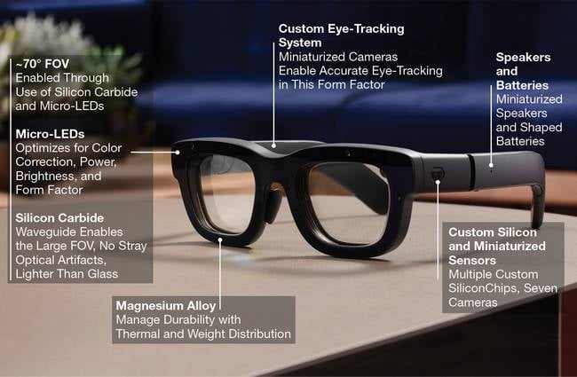
Meta’s 2024 demonstration of the usage of silicon carbide (SiC) as a substrate was highlighted by its Orion AR glasses protype, featuring a 70° FOV. Courtesy of Meta.
Regardless of the material polytype selected, electronics functionality depends on correct doping and induced defects. SiC is most often doped with carefully controlled proportions of impurities, such as nitrogen or phosphorus for n-type materials, aluminum or boron for p-type materials, and vanadium for semi-insulating functionality (where high resistivity is desired to isolate current flow between components for high-speed electronics3).
In optics and photonics applications, however, material purity is often the most essential determinant to low absorption losses. This makes optical-grade SiC an interesting and perhaps universal base substrate choice for the broadest applications where doping can be subsequently processed. Given this, it could be beneficial to localize both doping and defects so that electronic, photonic — and even quantum — processes would be possible on a singular substrate4.
AR and SiC: The next-volume wave
Advancements in the electronics industry increasingly rely on and highlight the distinct capabilities of SiC. Coupled with growing awareness and the development of higher-quality materials, this has spurred continued investigations into SiC’s optical and photonic properties. In October 2024, for example, Meta demonstrated the usage of SiC as a substrate for Orion, its 70° FOV augmented reality (AR) glasses prototype. Meta partnered with the existing base of industrial SiC material and device manufacturers to deliver this demonstration. The collaboration proved that optical-grade SiC substrates can be fabricated using established commercial means to reach the high optical transmission and tolerances required to create high-quality optical and photonics structures. These wafer substrates were processed using standard lithographic techniques to create the nanostructured gratings necessary for superior AR waveguides.
The development of the prototype validated the value of wide FOV AR glasses in a consumer-friendly form factor. This could present a major shift on the trajectory of SiC, the AR industry, and photonics. It is hard to explain the “wow” factor that users experience when donning a pair of AR glasses, for example, to convey the importance of a wide FOV that SiC enables. Perception — the fundamental quality on which AR relies — is itself a personal perspective. And future commercial success of AR devices will ultimately hinge on factors such as space constraints, social acceptability, portability, and cost.
Additionally, considering historical consumer behaviors toward televisions, computer monitors, and mobile devices, it is reasonable to expect that many consumers will want a larger display if there is not a corresponding sacrifice to other important product attributes.
But even against this backdrop, it is obvious that a wide FOV provides world-locked digital content to remain in a wearer’s FOV when they reposition their heads, bodies, and eyes. This is a fundamental difference between “information” or “smart” displays and full AR, in which contextual objects can be overlaid on top of the real world to increase our hybridized perception in a meaningful way. While both experiences have value, full AR’s experience exceeds what any display system or human computer interface has yet achieved in an always-available format. In this context, Meta’s Orion prototype demonstration is positioned to represent a milestone for the future of AR devices and their architectures.
Additionally, considering historical consumer behaviors toward televisions, computer monitors, and mobile devices, it is reasonable to expect that many consumers will want a larger display if there is not a corresponding sacrifice to other important product attributes. It therefore seems possible, and even likely, that the rollout of AR glasses will begin with small displays, though once a wide FOV display is commercially mature, a sizable proportion of wearers will migrate toward this enhanced experience. The significance of this pivot is difficult to predict. The profound shift from mobile phones to smartphones could offer context.
In all waveguide-based AR displays (including Meta’s Orion prototype) two factors fundamentally limit the FOV of the system.
First is the overall display efficiency. A combination of the waveguide and projector engine electrical-to-optical efficiency to the eye, within the allowable optical system etendue, dictates this efficiency. The system’s thermal (head dissipation availability) and power density given a weight constraint limit the FOV.
The second factor is a limitation of the optical system etendue itself, which is controlled by the difference in the index of refraction between the waveguide substrate and its interface, commonly air or a low-index material. The higher the index difference between these interfaces, the greater the angular acceptance of the optical system — and the freedom for waveguide or grating designers to balance key image trade-offs. Waveguide designers, as is true of lens designers, must trade performance parameters in addition to cost and complexity. In waveguide design, these parameters include off-color uniformity (corrected by imager calibration, though at the cost of efficiency losses), modulation transfer function, ghosting, overall efficiency, and front side grating leakage to the outside world. Another parameter is rainbow artifacts. These are especially troubling for all-diffractive waveguides. They describe the coupling of outside light sources into the waveguide diffraction gratings and the dispersive release of light within the wearer’s FOV. These rainbow artifacts move and change with the wearer’s positioning relative to the light sources.
In the case of the Orion demonstration, the displays are three tiny micro-LED projectors. These elements deliver red, green, and blue optical pupils that each advance through a diffractive input coupler fabricated as a surface relief grating that feeds the image into the SiC substrate to support total internal reflection. The total internal reflection replicates the optical pupils and presents these multiple pupils onto the output face of the substrate that contains a diffractive output coupler to deliver light into the eyes regardless of location. This substrate makes up a portion of the lens structure of glasses.
A second output grating is built onto this surface and selectively couples pupils out to present an eye box within which the wearer receives the light regardless of eye position. SiC’s high index of refraction between 2.6 and 2.7 in the visible range enables the substrate to support a larger total internal reflection angular range inside the substrate and a >70° diagonal FOV as well as the large required etendue.
Designers are also able to leverage the increased bending power associated with this high index of refraction to shift the rainbow positions toward the edges of the FOV. This serves to reduce the effect on the wearer. In fact, it becomes possible to eliminate most obtrusive rainbows with an index of refraction roughly >2.5. This makes SiC, with its high index of refraction in the visible range, an optimal substrate choice regardless of the FOV: Alternate material options such as high-index glasses and lithium niobate will retain rainbow artifacts in such conditions.
Material and supply chain considerations
Beyond material properties, considerations given to the scaling and development of existing supply chains and associated cost reductions are critical to a mass adoption of optical-grade SiC by the optics and photonics industries, starting with the AR sector. For this mass adoption to take place, the specifics of an ideal supply chain must be determined. First, it must facilitate the reliable delivery of both substrates and completed waveguides at a consumer-friendly price. This requires a mental and business shift away from electronics with scaling small devices toward optics with relatively large components. AR waveguides are ~50 mm diagonal, with two required per pair of glasses. Therefore, even a small consumer volume of glasses of 1 million pairs requires roughly 300,000 substrates with somewhere around four pairs of lenses per 200-mm wafer.
This math presents an important opportunity for SiC substrate manufacturers to diversify their business. The importance of a diverse customer portfolio has become apparent as the growth of the power electronics business slowed through 2024, along with an unanticipated decrease in the rate of electric vehicles sold and infrastructure conversion in Europe and North America. This has left SiC capacity underutilized, with many prepared facilities available or ready to scale, but paused.
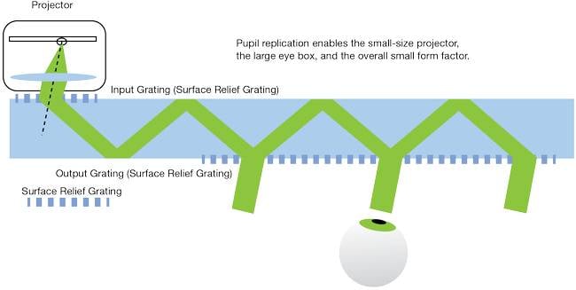
Waveguide functionality gauged by its effect on the human eye. Meta’s Orion demonstration featured a prototype with three micro-LED projectors. A diffractive input coupler, fabricated as a surface relief grating in the silicon carbide (SiC) substrate, supports total internal reflection until it is released to the eye by a surface relief grating output coupler. Courtesy of Meta.
Additionally, pricing pressure has appeared for electronics substrates. This has closed some of the pricing gaps required to support consumer AR waveguides. The release of the Orion prototype and momentum stemming from it has enlivened and engaged the SiC supply chain toward developing and scaling optical-grade SiC. The timing of this transition may indicate ideal conditions to seed the initial launch of wide FOV AR glasses starting with 200-mm infrastructure and rapidly moving toward 300 mm to increase volumes and further lower costs.
Driving electronic-photonic convergence
Though challenges in moving toward mass adoption are real, they are no longer wholly technical problems. Rather, they are more precisely defined by engineering and business concerns. History — specifically in solar panels and batteries, both characterized by massive price drops during the last decade — has shown that these concerns can be overcome when large markets are involved as processing and material developments progress. The speed of such changes is typically driven by collaborations between academic, industrial, and government agencies engaging in parallel to drive the inevitable changes.
It is also a safe assumption that the volume and quality of SiC material will continue to improve from the planned investments. Higher-purity materials will spur a second push toward even better electronics and a new market of wide FOV AR displays.
The individual next steps of the transition toward SiC are more speculative, though equally compelling. Many photonics researchers began their work with SiC even before the availability of optical-grade substrates. This provides some context for the R&D undertakings that have demonstrated many different active and passive photonic devices, including beamsplitters, polarization beamsplitters, optical switches, combs, and micro-ring and micro-disk resonators. Also, selected material defects in SiC crystal structures have been demonstrated to support the creation and addressability of single photon sources for quantum computing. Now, localized doping and defect treatments, along with nanofabrication processes of coating, etching, stacking, and more, could enable a convergence of electronics, photonics, and quantum photonics, all sharing a common substrate to seamlessly mate cross functional platformed integrated circuitry and computing.
It is obviously interesting to hypothesize about a future self-reinforcing ecosystem creating a path for combined integrated optoelectronics around SiC. Currently, massive gains in AI infrastructure and quantum computing breakthroughs are defining the technology landscape. Should quantum supremacy be validated, scaling is anticipated to begin, with efforts guided toward applying this computing toward AI inference and training. This will require a low-cost electronic-to-photonic and quantum-supporting infrastructure.
Meanwhile, AI computation is already scaling, with data processing requiring enormous infrastructure investments of servers as well as the power systems to support them. This will make efficiency even more important than it is currently. And, it will further drive research and increase the business of SiC electronics.
AR glasses will be a major user of the AI infrastructure as training on live contextual information becomes necessary and the resulting information is delivered on SiC-based wide FOV glasses. Perhaps quantum computing on SiC will eventually deliver the next AI infrastructure buildout that feeds this future of wearable computing.
This is not unlike the self-fulfilling circular ecosystems, driven by the solid-state transistor integrated circuit toward computing, that have led to both display and AI.
But now, if this occurs again, electronics, photonics, and quantum physics will have merged.
Acknowledgments
The author wishes to recognize Victorian Miniere, Pasqual Rivera, Giuseppe Calafiore, and the Orion Waveguide team for their contributions to the technology and work described in this article.
References
1. V. Veliadis et al (2024). Overview of silicon carbide. In: Sic Technology: Materials, Manufacturing, Devices and Design for Power Conversion. M.D.P. Emilo, ed. Springer, pp. 1-23.
2. TrendForce. How many 8-inch silicon carbide wafer fabs are there worldwide? www.trendforce.com/news/2024/10/14/news-how-many-8-inch-silicon-carbide-wafer-fabs-are-there-worldwide/.
3. H. Xiong et al. (December 2022). Characterizations on the doping of single-crystal silicon carbide. Mater Tod Phys, Vol. 29, 100906.
4. K. Speer et al. (2024). SiC material properties. In: Sic Technology: Materials, Manufacturing, Devices and Design for Power Conversion. M.D.P. Emilo, ed. Springer, pp. 25-66.