Board-level technology and improved interface capabilities enable the analysis of data during industrial processes, security surveillance, and environmental monitoring.
Embedded cameras, often called board-level cameras, may measure only a few centimeters in width, but they represent a key element in the evolution of machine vision capabilities. With improvements in sensors and interfaces that boost the amount of data that can be transferred in brief intervals, these devices are being placed not only in systems that evaluate quality on the industrial floor but also in systems for security monitoring, agricultural inspection, and medical examination.

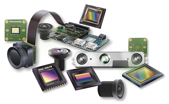
An embedded imaging system helps in the inspection and harvesting of crops. Courtesy of FRAMOS GmbH.
The marketplace shift to using this technology has been driven in part by the mobile phone market. Whereas the first camera phones were introduced with little fanfare 25 years ago, modern smartphones have shaped imaging as well as data processing. As sensors and microprocessors become more efficient and powerful, the companies that produce mobile devices are able to provide a hand-held product such as a tablet or smartphone that enables not only using more megapixels in an image but also placing sensors that can capture details in a particular setting. The placement of this improved sensing capability includes applications in areas such as gesture and face recognition and the tracking of particular features in man-made or natural products.
At the most basic level, an embedded camera is essentially a sensor, lens, and interface mounted directly onto a circuit board, along with electronics that power and regulate the imaging. While either CCD or CMOS sensors can be used, CCD technology is being phased out, and CMOS sensors are found in newer systems. CMOS sensors are preferable due to their smaller size, lower power consumption, and higher performance for most embedded vision applications.
The camera module sometimes contains an image signal processor chip, or ISP that may improve image and color quality. For example, the ISP sharpens and denoises the image, and it demosaics the data, meaning it reconstructs a full-color image from a GGB Bayer-filtered pixel arrangement. However, many embedded vision platforms have ISP functionality on the main processor board, and, in this case, the module outputs a raw image captured by the sensor. Features such as high dynamic range and triggering capabilities can be added into the sensor itself.
Cameras containing such sensors are widely used for consumer products or other fixed applications, such as surveillance services. However, industrial applications usually require raw data from the sensor to avoid distortion of the data and to allow for application-specific image data processing and analysis.
Various lenses are incorporated into the camera, depending on sensor and pixel sizes. “The lens defines the field of view, that is, what the camera sees,” said Gion-Pitschen Gross, director of product management and marketing for Allied Vision Technologies. “The lens also defines the working distance, which is the distance from the object to the camera and that is needed for focusing.”
Prashant Mehta, senior field applications engineer at FRAMOS, said the Sony sensors placed in the company’s sensor modules range from 0.4 to 24 MP and higher resolution. Lower-resolution sensors, such as 0.4 and 1 MP, are best suited for high-speed factory automation applications or barcode scanning. He said 8- to 12-MP variants are for 4K video generation, such as professional video and sports event recording.
“Anything higher resolution-wise is useful, depending on the applications, such as inspection of high-density printed circuit boards, professional video capture applications, very high-end surveillance, aerial photography, and so on,” Mehta said.
In older CCD sensor-based systems, he said, tens of watts were required to provide power for a variety of components, whereas with CMOS technology it is possible to create a system on a chip (SOC) that reduces power needs to 1.2 or 1.8 V. This reduction is advantageous for mobile applications when battery power is limited, such as when facial recognition is performed in busy settings, or when drones are used for substantial flight time.
“Five years ago, the big push for embedded cameras came from security and machine vision,” Mehta said. These applications require multiple viewing perspectives, as well as synergy between sensors. “Now, the CMOS sensor technologies previously reserved for digital cameras and mobile phones has become widely available on off-the-shelf sensors. The miniaturization of the components has helped bring costs down.”
Companies offering embedded or board-level cameras often differentiate products based on processing capabilities.
“For Basler’s embedded MIPI [mobile industry processor interface] cameras, it is important to know that the camera logic that runs on the target processing platform must also be considered to be part of the whole image processing system,” said Florian Schmelzer, a product marketing manager with Basler AG. “By transferring the camera logic from the camera to the processing system, it is possible to come to extra lean and cost-efficient designs.”
With a MIPI interface, many cameras (whether high- or low-resolution) can be connected to an image signal processor. And with features such as a smart region of interest for inferencing, the number of conduit wires is reduced. Many sensors can be connected to a mobile SOC. Embedded vision designs allow for integration of the system into OEM environments that are space constrained and have power limitations.
Speed and power
Historically, the trade-off for the reduced size and potential integration of embedded cameras into an overall vision system was the inherent limitation on camera speed and image resolution. But these barriers have come down.
Speed and resolution are only limited by the interface, Schmelzer said. In the case of MIPI cameras, recent specifications allow for a bandwidth of 2.5 Gbit/s per lane or channel. If the sensor has four lanes, the transfer increases to
10 Gbit/s per lane. This increase translates into more than 60 fps at 4K pixel resolution at a 2-byte pixel format, which could be useful in security surveillance or driver assistance systems, which need to authenticate information as quickly as possible.
“For leaner pixel formats you can easily achieve 4K pixels with up to 120 fps,” Schmelzer said. “However, today only a few sensors support such a high speed, and only a few target processing platforms allow for 2.5 Gbit/s per lane.”
Vision Components offers MIPI camera modules with a large range of image sensors and many processing platforms that can fit into applications for industrial and consumer-oriented products. “The MIPI CSI-2 interface has become a standard interface and is supported by many CPU boards from NVIDIA, NXP, and numerous other leading manufacturers,” said Jan-Erik Schmitt, vice president of sales at the company.
This standardization was driven by high-volume markets such as smartphones and other mobile applications in the consumer market, wherever more cameras have been deployed that utilize the interface. As a consequence, modern CPU boards also widely support the MIPI CSI-2 interface. MIPI camera modules cater to the high demands in professional applications due to their high-end image quality, robust design, longevity, and long-term availability.
And while higher speed and resolution could potentially lead to higher power needs, companies such as Allied Vision try to incorporate intelligent features that power down parts of the camera to conserve energy when the camera does not need to run at full speed.
New applications
Elements such as high resolution and high dynamic range combine to enable placement of embedded cameras in applications in which high throughput and accuracy are essential, and in settings in which they may not necessarily have functioned well in the past. Schmelzer gave the example of intelligent traffic monitoring systems, which need to function in widely varying conditions.

Components of an embedded imaging system. Courtesy of FRAMOS GmbH.
One the one hand, there can be glistening daylight, and on the other, the system can be faced with twilight situations in which both poorly visible pedestrians and a passing car with glaring headlights are present,” he said.
Powerful embedded CPU boards and versatile MIPI cameras combine to replace traditional systems that have external cameras and PCs. All-in-one systems are ultracompact and cost-effective due to reduced overhead, and they can be tailored to specific applications. By utilizing technologies such as onboard image processing units and AI-accelerators based on field-programmable gate arrays (FPGAs), these systems meet the high demands for edge computing devices.
For higher levels of integration, the camera modules can be soldered directly to a CPU board, along with all the components needed for image acquisition and analysis. Embedded vision systems with onboard image sensors or MIPI modules integrated as remote-head sensors are placed in drones, security and surveillance applications, traffic systems, and point-of-care diagnostic devices. An FPGA-based hardware accelerator can also be integrated into MIPI data streams flowing from the camera to the CPU board, which enables complex image processing.

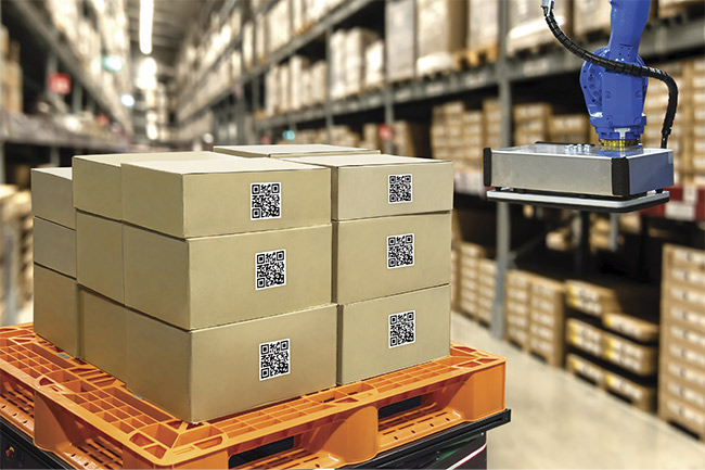
An embedded camera facilitates smart materials handling. Courtesy of FRAMOS GmbH.
According to Mehta, machine vision applications in which an embedded camera would be used are dominated by metrology and defect detection, such as taking high-resolution pictures of a recently manufactured part, or in automatic optical inspection.
Applications are also deployed to measure the part (such as its feature locations and dimensions) and/or detect defects. “That’s when machine learning comes into the picture,” Mehta said. “This can track defects. Similarly, higher-resolution imaging can be useful for novel applications like digital pathology. Traditionally, a pathologist may only look at several areas of a slide. With the aid of computer vision, the software can identify areas of interest and help the pathologist cover the entire slide to make a better-informed decision.”
Meanwhile, the expansion of the wavelength range of embedded cameras into the NIR and SWIR ranges has also opened up the potential for applications where more than just visible light is required, said Allied Vision’s Gross. The NIR range is between 750 and 1000 nm — invisible to the human eye — and SWIR is between 1000 and 2500 nm. Sensors for the two require different technology.
“NIR image sensors are based on standard silicon technology like normal image sensors are,” he said. “NIR technology is used a lot in positioning or 3D applications, together with structured light. Invisible light patterns are shined onto objects and the detailed shape or position can be reconstructed from the deformation of said patterns.”

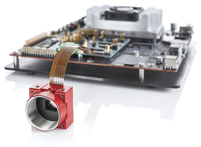
The opening housing of an Alvium carrier board. Courtesy of Allied Vision.
Embedded cameras are still useful on the production line, Mehta said, where an issue needs to be flagged immediately. And the cameras are also finding home security applications, in systems (aided by machine learning) that need to flag certain objects and not others.
“There are security applications where an element should trigger an alarm or send a call to the owner, and times that it shouldn’t,” he said. “The camera can even be put on a helicopter and be used in everything from wildlife conservation to border security.”
An Eye for Vision
AI has been central to advancements made in the embedded vision systems that are the core market for Prophesee, a corporate spinoff of the Vision Institute in France. Though the company does not specifically build cameras, it built a sensor that is compatible with vision systems and that is designed to mimic the human retina and the way the eye acquires information. The company designed software equipped with algorithms to support the construct. It then created toolkits for incorporating the combined technology into vision systems. And the sensor and software can function with MIPI and USB cameras.
“We don’t have a rolling or global shutter, or even a frame rate, because our technology isn’t based on images,” said Guillaume Butin, marketing communications director at Prophesee. “The photodiode captures the light, but each pixel in the sensor has its own logic.”
The technology is called event-based vision. The sensor has the ability to turn on or shut off depending on movement or other factors. But when a camera with this sensor is running, it is able to see between the frames that another camera would capture individually, Butin said.
“Our sensor operates in the 10,000-fps equivalent time resolution range, while not being limited by exposure,” he said.
The next step in using the technology involves embedding it within a vision system, where it could help filter out flickering and noise, depending on the needs of a particular application. Because an event-based system is not capturing thousands of images and processing them, it can detect problems far sooner than other systems may be able to, such as during welding. Such detection could facilitate predictive maintenance.
Most of the company’s customers are located across the U.S., in the European Union, and in China, while its three core markets include the needs of Industry 4.0, the mobile Internet of Things, and automotive (both safety- and non-safety-related systems).
“A camera with this technology could monitor particle or object size very fast, as well as object tracking,” Butin said. “We successfully counted and sized objects at up to 500,000 pixels per second. At the same time, it natively segments a scene at the pixel level. It is only analyzing motion, as opposed to the road beneath, for example.”
Prophesee is working with the automotive sector to develop event-based lidar systems. The company is also collaborating with other industries to produce AI-based systems in goggles to potentially restore sight in people affected by vision loss.
But regardless of the setting, the lack of dependence on frame grabbing or massive data processing has resulted in a market for the company’s technology, Butin said. “This event-based sensor has enabled lower power consumption and allows placement in settings that have limited power.”