Jens Hashagen, Allied Vision Technologies GmbH
Infrared imaging opens endless possibilities for industrial, scientific and security image-processing applications. But short-wave infrared cameras must overcome the limitations of InGaAs sensor technology to provide high-quality images.
Conventional imaging sensors such as CCD or CMOS have a wider sensitivity range than the human eye, especially in the near-infrared area. They reveal more than the bare eye can see. For example, an easy way to check if an infrared remote control is working is to operate it in front of a digital camera. The IR signal is visible on the image as a flash of light.
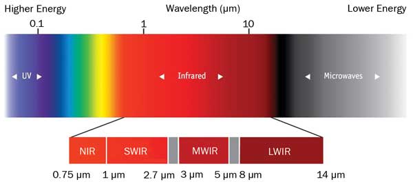
The infrared spectrum. Images courtesy of Allied Vision Technologies GmbH.
Other sensor technologies make it possible to image deeper into the infrared spectrum – but that spectrum is far wider than the visible range. It is therefore commonly divided into subcategories that require different imaging technologies. The wavelength definition of these categories is not normed but is widely accepted within the imaging sensor industry:
• Near-infrared (NIR): 0.75-1 µm
• Short-wave infrared (SWIR): 1-2.7 µm
• Mid-wave infrared (MWIR): 3-5 µm
• Long-wave infrared (LWIR): 8-14 µm
• Ultralong-wave infrared (ULWIR): 14-30 µm
These different spectral ranges require specific sensing technologies to detect infrared radiation in their respective wavelengths. Besides NIR, SWIR is the bandwidth most widely used for industrial and scientific applications.
SWIR imaging: wide applications
Short-wave infrared cameras enable various new applications or enhance current machine vision systems by imaging beyond the visible spectrum. As an example, seeing through surfaces that are nontransparent to the human eye helps users visualize underlying features such as fill levels, hidden moisture or tamperproof security codes.
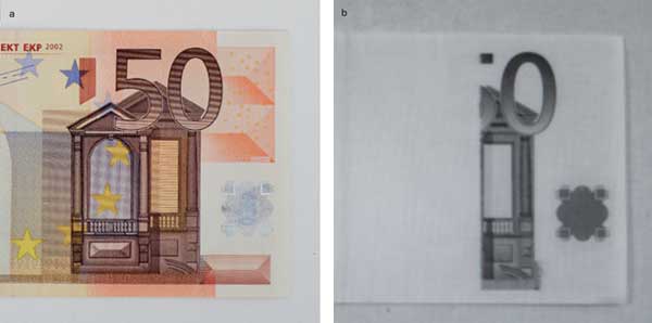
Banknotes shown under (a) visible and (b) IR light.
Additionally, using filters, wavelength-optimized optics or monochromatic light sources is convenient for capturing a distinct and a measurable contrast of the inspected object.
A popular SWIR application is moisture detection. Water is transparent to visible light, but it absorbs strongly at wavelengths of 1450 and 1900 nm, which makes it appear black in the image. With a corresponding filter or lighting, this ability can be used for various inspection tasks in the food and beverage, woodworking, textile or automotive industries: Examples include verification of coatings or dryness uniformity in bulk material, fill-level detection through nontransparent containers, detection of damaged or bruised fruit, and gauging relative water content in plants.
Other materials are opaque in visible light but transparent to infrared radiation. This property can be used for the nondestructive inspection of products. For example, SWIR cameras are used by syringe manufacturers to automatically check the presence of the needle by imaging through the protective cap:

Optimization of an InGaAs sensor image in a SWIR camera.
The plastic of the cap is IR-transparent, while the metal needle is not. Art historians use SWIR cameras to visualize pencil or charcoal drawings beneath the paint layers of artwork, and infrared-transparent inks are used to certify the authenticity of banknotes or other valuable documents.
SWIR cameras can also be used for spectroscopic analysis; examples include structural clarification of unknown substances, categorization of purity of substances, plastics sorting for recycling, or quality analysis of agricultural products. Spectroscopy is nondestructive and, in general, requires no sample preparation. Therefore, many material attributes can be inspected rapidly in-line for qualitative, as well as quantitative, parameters.
In wafer and solar cell production, electroluminescence is used especially in the final production step of quality inspection to detect microscale cracks and printing problems. Photoluminescence, in turn, can be applied throughout the entire manufacturing process. SWIR cameras are most qualified for these tasks because the light emitted by silicon has a peak at ~1150 nm. Moreover, the quantum efficiency of InGaAs sensors (starting at 900 nm) is much higher (>70 percent at 1050 nm) than NIR-enhanced cooled or uncooled CCD and CMOS cameras (<10 percent at 1050 nm), which cannot detect wavelengths above 1100 nm because silicon is transparent beyond this wavelength. Therefore, SWIR cameras are perfect to image through the wafer to detect metallization and electrical-contact defects.
Overcoming InGaAs sensors’ weaknesses
For these applications, SWIR cameras must output images of a quality high enough that people or machines can analyze them accurately. This is a technical challenge because of the nature of InGaAs sensors.
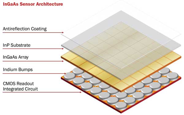
InGaAs sensor architecture.
Sensors used in SWIR cameras function similarly to silica-based CCD or CMOS sensors by working as quantum detectors, converting photons into electrons. But to detect light beyond the visible spectrum, their photon-sensitive area is made of materials such as indium gallium arsenide (InGaAs) or mercury cadmium telluride (MCT or HgCdTe). Depending on the material’s chemical structure, these sensors are sensitive to different wavelength ranges and might require strong cooling to achieve a proper signal-to-noise ratio (sometimes down to cryogenic temperatures, using liquid nitrogen or a small Stirling cycle refrigerator unit). The most commonly used sensor technology in the SWIR spectrum is InGaAs because it does not necessitate cryogenic cooling, which makes it more practical and affordable than MCT.
Unlike silicon-only based CCD and CMOS sensors, an InGaAs sensor has a hybrid architecture that combines a silicon-based CMOS readout circuit with an InGaAs photosensitive array. The InGaAs device is normally grown on an indium phosphide (InP) substrate; its thickness and the ratio between indium (In) and gallium (Ga) will influence the wavelength sensitivity of the sensor.
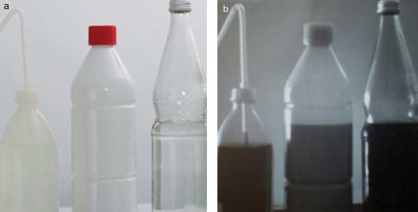
Bottle fill levels shown under (a) visible and (b) IR light.
Combining the InGaAs array with the readout circuit is a relatively complex and time-consuming process, as many manufacturing steps are needed. Additionally, the production yield is relatively low. All this makes these sensor types more expensive than CCD or CMOS sensors.
In spite of their relatively high cost, InGaAs sensors are far from being perfect. Currently, it is technically impossible to combine the readout circuit with the photosensitive area with 100 percent accuracy and uniformity. Consequently, compared with CCD or CMOS sensors, these sensors inevitably have a small percentage of defective pixels (<1 percent). In addition, each pixel shows a slightly different behavior. Without any image preprocessing inside the camera, the raw image looks noisy.
Fortunately, camera manufacturers implement various techniques to optimize the image quality before it is transmitted to the image-processing system.
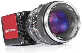
The Goldeye from AVT uses image optimization for a variety of imaging applications.
The following example describes how the Goldeye SWIR camera series from Allied Vision Technologies tackles optimization: Sensor cooling is the first thing required to optimize the image. The camera features a built-in sensor-cooling and temperature-control system using a Peltier element to ensure that the sensor temperature remains constant at a low level. This reduces the dark noise and allows longer exposure if the application requires it. A second step consists in applying preprocessing algorithms to correct the sensor-inherent anomalies of the image: Nonuniformity corrections remove artifacts generated by the nonuniform photosensitive response of each pixel part of the InGaAs array and its underlying structure. Defective-pixel correction removes defective pixels – dark (cool), blinking and bright (hot) pixels – from the image by replacing them with a value extrapolated from the brightness of neighboring pixels.
SWIR imaging offers many opportunities for advanced image processing applications. However, InGaAs sensor technology does have its limitations, and these show up across all camera vendors. A camera’s actual image quality very much depends on the expertise of the camera manufacturer in optimizing the image by use of sensor cooling, sensor temperature monitoring, and image correction inside the camera.
Meet the author
Jens Hashagen is a product manager at Allied Vision Technologies GmbH in Stadtroda, Germany; email: jens.hashagen@alliedvision tec.com.