Researchers Remove Obstruction to Single-Photon Emission in Quantum Dots
Quantum dots (QDs) are an efficient interface between matter and light and could potentially form the basis of quantum communications. However, their signal can be obstructed by structures that form by default during their manufacture. Researchers at the University of Basel, Ruhr-Universität Bochum, and Forschungszentrum Jülich have found a way to eliminate these interfering structures.

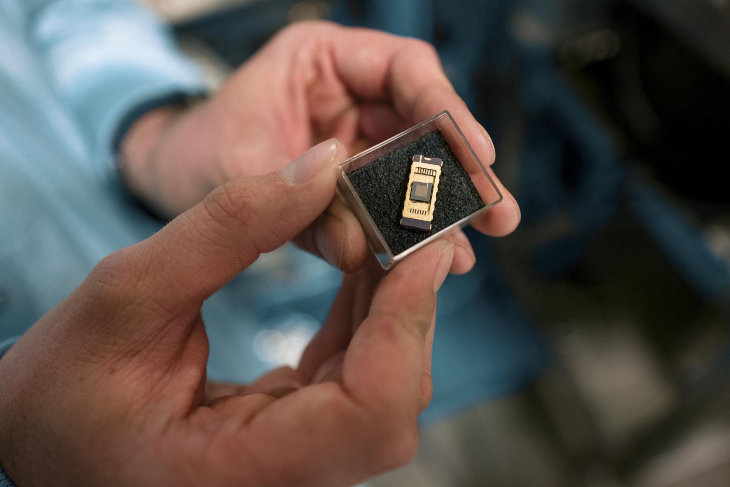
The Bochum team at the Chair for Applied Solid State Physics realizes quantum dots in semiconductors. Courtesy of RUB, Kramer.
The QDs manufactured in Bochum are generated in the semiconductor material indium arsenide (InAs). The researchers grow the material on a gallium arsenide (GaAs) substrate. During this process, an InAs layer forms at a thickness of 1.5 atomic layers; this is called the wetting-layer. Subsequently, the nm-size quantum dots are generated.
The wetting-layer results in a continuum that is close in energy level to the confined states of the QD, and this leads to scattering and dephasing of the QD-excitons. In the wetting-layer, exciton states decay even more easily than in the QD. The photons emitted in this process can’t be used in quantum communication; they would generate a static noise in the system.
“The wetting-layer covers the entire surface while the quantum dots only cover a 1000th of the semiconductor chip, which is why the interfering light is approximately 1000 times stronger than the light emitted by the quantum dots,” professor Andreas Wieck said. “The wetting-layer radiates photons at a slightly higher frequency and at a much higher intensity than the quantum dots.”
Charging QDs with electrons could potentially improve their ability to carry information for quantum applications. “But in that case, the energy levels in the wetting-layer would be likewise excited,” researcher Arne Ludwig said.

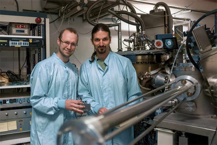
Sven Scholz (l) and Arne Ludwig generate quantum dots in semiconductors. Scholz was awarded with a dissertation prize by the Wilhelm and Else Heraeus Foundation for generating the sample. Courtesy of RUB, Kramer.
To remove the interference caused by the wetting-layer, the researchers modified the growth-protocol of InAs on GaAs. They added an aluminum arsenide (AlAs) layer, which was grown above the QDs in the wetting-layer. The additional layer eliminated interferences by removing the energy states in the wetting-layer and thus making it less likely for electrons and electron holes to recombine and emit photons.
The researchers demonstrated that the new QDs had no wetting-layer-continuum for electrons and could host highly charged excitons, where up to six electrons occupied the same QD. According to the team, single QDs grown with this protocol exhibit optical linewidths matching those of the best QDs, making them an attractive alternative to conventional InGaAs QDs.
The research was published in Communications Physics (https://doi.org/10.1038/s42005-019-0194-9).
Published: September 2019