Left-handed materials — materials with a negative refractive index — continue to be a focus of investigators in pursuit of “superlenses” and other novel device designs.
Hank Hogan, Contributing Editor
Researchers are considering the optical equivalent of the Zen koan about the sound of one hand clapping. In optics, however, there’s a twist: It isn’t the use of two hands that is the norm. Typically, such widely used applications and components as photolithography and radio antennas have relied on the effect of only one electromagnetic hand clapping.
In nature, there are only “right-handed” materials, which have a positive refractive index and for which the right-hand rule governs the direction of electric and magnetic fields with respect to the direction of propagation of an electromagnetic wave passing through the material. Now scientists are building negative refractive index materials — “left-handed” materials for which the right-hand rule is replaced with its left-hand equivalent — of metallic nanostructures and photonic crystals. If the practical problems involving their construction for visible light can be overcome, the applications might include optical nanolithography, beam steering and better biomolecular imaging. In other parts of the electromagnetic spectrum, applications could include waveguides and antennas for radio and microwaves that are smaller than has been possible.
“This is one of the most exciting developments in optics, and it might have a revolutionary impact,” said Vladimir M. Shalaev, a professor of electrical and computer engineering at Purdue University in West Lafayette, Ind., who will be co-chairman of a conference on photonic metamaterials in June 2006. Metamaterials are built of structures that are much smaller than the wavelength of interest, and they are one of the leading candidates to achieve negative refraction in the visible.

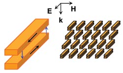
A group from Purdue University employed an array of 120-nm-wide, 670-nm-long gold nanorods spaced 60 nm apart to achieve negative refraction at a wavelength of 1.5 μm. However, practical problems must be considered and overcome before negative-index materials are put to use. Also, some of the predictions involving these materials are controversial. In particular, there has been an ongoing dispute in the research community as to whether it’s possible to build a “superlens,” a left-handed lens that can image subwavelength-size objects at a distance. That debate may be dying down, with the superlens proponents seeming to have carried the day.
The refractive index of a material is a function of its electric permittivity and magnetic permeability relative to vacuum. The change in refractive index causes light to bend as it moves from glass, which has an index of 1.45, to air, with an index of nearly 1. As it turns out, it is possible to build left-handed materials that have negative permittivity and permeability. Such materials have a negative index of refraction, and lenses built of them bend light in a direction opposite to that of an everyday lens of the same shape.
Although the idea had been around for decades, no one had an inkling of how to build a material with a negative refractive index. Then, in 2000, John B. Pendry of Imperial College London published a paper outlining an approach that has been widely adopted. He suggested using an antenna structure based on split-ring resonators to achieve negative permeability. David Smith and Sheldon Schultz of the University of California, San Diego, showed that this technique works with microwaves, achieving negative refraction.
The method employs surface plasmons — electron oscillations on the metal’s skin — and the spacing of the antenna elements. The spacing determines at what wavelengths the metamaterial exhibits negative refraction. Smith and Schultz used structures that were relatively large, so their metamaterial showed negative refraction only in the microwave region. Shalaev and his group at Purdue recently used a structure based on parallel gold nanorods, 120 nm wide and 670 nm long and spaced 60 nm apart, to achieve a refractive index of –0.3 at a wavelength of 1.5 μm.
In theory, then, it’s possible to make a metamaterial that would have a negative refractive index in the visible spectrum — if one can fabricate small enough elements of the structure. In practice, however, that’s not easy.
Loss and other problems
The metal-based method can lead to such large losses that only a small fraction of the photons that enter the material make it out. It’s as if a lens maker had only very dark glass with which to work. That problem might be cleared up using some clever designs. Another approach, however, might be to use photonic crystals. The losses for such structures are small because they are built of dielectrics.

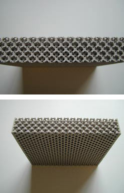
Using two- and three-dimensional photonic crystals, researchers from the University of Delaware demonstrated negative refraction at microwavewavelengths. The crystals consist of 20 layers. By scaling down the size of the unit cells, the scientists believe they can achieve negative refraction in the optical range. Courtesy of Zhaolin Lu.
At the University of Delaware in Newark, researchers recently used a three-dimensional photonic crystal to create a flat spherical lens that works by fully three-dimensional negative refraction at microwave frequencies. The crystal has 20 layers, each measuring 6.35 mm in depth, and was constructed using a technique the group developed.
“The fabrication is not too challenging but quite time-consuming,” said electrical and computer engineering graduate student Zhaolin Lu, who worked on the project with Dennis W. Prather’s group. “In the fabrication, the alignment accuracy is controlled to ±0.2 mm, which is quite small compared with the lattice constant of 6.35 mm and the wavelength.”
Studies by the scientists indicated that they had achieved subwavelength resolution, a benchmark of success, at frequencies of 16 to 17 GHz (wavelengths of 17.6 to 18.8 mm). Lu thinks the technique could be extended to infrared and visible radiation. As a matter of fact, the structure used was initially proposed for near-infrared applications. The difficulty was that the intricate structure couldn’t be built.
“The material is not problematic,” Lu said, citing the fact that materials such as germanium have a refractive index of 4.2 at a wavelength of 1550 nm. Prather and his group hope to push the wavelength down to the visible by developing and employing advanced fabrication techniques.
omes to a negative index of refraction. Because they’re composed of elements that are about the size of the wavelength of interest, they may be able to go negative for only a limited range of angles or over a limited range of wavelengths.
The other drawback, which holds for all negative-index materials, is a consequence of negative refraction itself. These materials are highly dispersive, so their refractive index depends strongly on wavelength. A material with a negative index at one wavelength may have a positive index at another. Indeed, all left-handed materials demonstrated to date have a positive index at some wavelength. This wide variation could enable entirely new applications while making the design of a lens and associated optical system tricky.
Perfecting lenses
These challenges haven’t dissuaded researchers, and for good reason. When Pendry outlined how to achieve a negative refractive index, he made another prediction: If an index of 21 could be attained, the result would be a so-called “superlens,” for which the resolution limit wouldn’t be the wavelength of imaging light but rather would be determined by the material itself. In theory, it is possible to achieve nanometer resolution using visible light.
A superlens would have a number of important applications. Semiconductors are built using photolithography. The industry spends huge sums developing and deploying tools to image ever-smaller features, which measure a few tens of nanometers in state-of-the-art processes. Being able to use an optical laser would eliminate the need for more exotic sources.
Likewise, the study of biological molecules for both research and diagnostics would benefit from subwavelength resolution. Today, many of the most interesting aspects of biology are hidden by the diffraction limit. Another fruitful area involves optical data storage, where being able to write and read smaller features would boost capacity.
Nobody has built a far-field superlens yet, but this capability has been demonstrated in near-field setups in which the object to be imaged and the image itself are closer to the lens than a wavelength of light. Two teams, one working at the University of Canterbury in Christchurch, New Zealand, and the other at the University of California, Berkeley, accomplished this using a thin layer of silver.
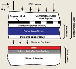
According to Richard J. Blaikie, associate professor of electrical and computer engineering at the University of Canterbury, the key to the technique lies in achieving a very flat surface. His group’s experiment involved a 50-nm-thick silver layer that had a roughness of about 1 nm. He and graduate student David O.S. Melville found that a 365-nm source could image features down to 145 nm, well below the conventional resolution limit of 243 nm. And, he noted, their work in this area hasn’t stopped.

At the University of Canterbury in New Zealand, a group broke the diffraction limit with a planar lens made of a stack with a 50-nm-thick silver layer, imaging 145-nm features in the near field with a 365-nm source. Theoretically, it may be possible to construct a “superlens” from left-handed materials that beats the diffraction limit in the far field.
“We are continuing to try and improve the resolution of the silver superlens, and have been making some good progress,” Blaikie said. He added that they also are looking into practical applications and potential patents.
Even without a working superlens, however, negative-index materials could be useful. For example, Joseph W. Haus, director of the Electro-Optics Program at the University of Dayton in Ohio, has been working on beam steering. Being able to switch a beam by changing the refractive index of a material has the advantage of altering the path of the light without resorting to mechanical means or to the conversion of the beam into and from an electronic signal.
This application doesn’t necessarily require a large change in the refractive index. By changing the index of a component material by a small amount, one could move a beam by changing the effective index by a large amount, Haus said.
Smaller devices
Another area that doesn’t require a superlens but that could benefit from negative-index materials involves waveguides and antennas for microwaves and radio waves. At present, waveguides are lossy if they’re smaller than the target wavelength and if they’re surrounded by lossy or thin cladding. With low-loss, negative-index materials, a waveguide could be made significantly smaller in cross section than the wavelength. That would allow devices to shrink.
Such longer-wavelength applications of left-handed materials are likely to appear first simply because the materials are easier to fabricate. The expectation is that other applications will follow. No one is sure of the time scale, but Shalaev said that he anticipates they will begin appearing fairly soon. He also said that, even if a superlens is never built, negative-index materials probably will have a large impact — in part because they provide novel properties and in part because refractive index plays a key role in so many areas.
The fact that the refraction can be moved to the new domain, to the negative values, opens new opportunities, he said.