A veritable explosion
of display-centric devices – new cell phones, handheld games, tablet computers
and televisions in a multitude of sizes and dimensionality (2-D, 3-D … n-D!)
is coming. Spurred on by ecologically minded consumers – and those wanting
long lives from their batteries – manufacturers are looking to replace power-hungry
displays with less ravenous new technologies. Now, displays enhanced by quantum
dots are getting an opportunity to grab their share of the limelight.
Not long ago, quantum dots were a rarely seen and very expensive
means of enhancing biological imaging. A painstaking blending of the right semiconducting
materials resulted in a small handful of very bright, regularly emitting particles
that could help track cell components or chemicals under the microscope. After a
few years of experimentation and development, quantum dot costs have come down enough
that their use is now growing.
Cost was a hurdle, but no one would be trying to incorporate them
into display technology if it weren’t for the benefits. Quantum dots, when
excited by electrons or photons, emit bright, steady light at a narrow wavelength
band and do so while drawing very little power. In comparison, organic LEDs are
even brighter and more efficient, but more expensive than quantum dot-based displays
project to be, especially at large sizes. Quantum dot displays promise to have longer
lifetimes as well.
Visionaries create future
One of the first private companies to dive into the field of quantum
dots was Watertown, Mass.-based QD Vision Inc. Over the past several years, the
company has been developing quantum dot technologies for use in novel low-power-consumption
displays. Achievements in this area resulted late last year in an agreement to help
LG Display of Seoul, South Korea, create direct-view active-matrix displays in which
quantum dots will help improve color brightness and saturation as well as energy
usage.
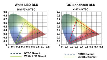
High-end LCD displays with integrated quantum dots will deliver
a 100 percent color gamut (versus the more typical 70 percent available today),
while maintaining lifetime, efficiency and other desired specifications of LCDs,
said Seth Coe-Sullivan, co-founder and chief technology officer of QD Vision (See Q&A on page 58).

Using quantum dots (QDs) in conjunction with LCDs produces more favorable color than unenhanced
white LEDs, while using about one-third less energy. BLU = backlight unit. Courtesy
of QD Vision.
“It is a little too early to put a specification on quantum
dot LED when it launches, but I expect the value proposition will be similar,”
he said. The ultimate goal is to “blow competing technologies away in terms
of color, make a marked improvement in power consumption and meet or exceed every
other spec.”
In January, QD Vision revealed that it had demonstrated a quantum
dot-based active matrix display that has an array of 800 x 600 pixels on a 15.6-mm-diagonal
screen. Designed under contract for the US Army, the tiny display will be a component
of video headsets, helmet-mounted devices and other instruments where the display
will be mounted near the eye. The demonstration model was an amber monochrome version,
but the company also is developing a full-color version.
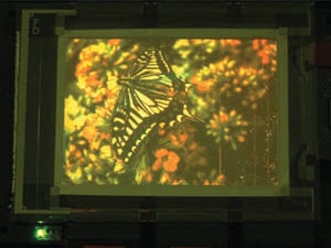
A month later, in February, Samsung Electronics’ Advanced
Institute of Technology in Yongin, South Korea, announced that it had developed
a large-area full-color display that incorporates quantum dots. The display measures
4 in. diagonally and comprises a 320 x 240-pixel array.

Researchers at Samsung have developed the largest QD-based display yet, a 4-in.-diagonal screen
with 320 x 240 pixels. Courtesy of Samsung Electronics.
In a paper published in the Feb. 20, 2011, issue of Nature Photonics,
Tae-Ho Kim and his colleagues first note that, although the availability of quantum
dots no longer is an issue, efficiently depositing them onto a glass or plastic
substrate has remained problematic.
A new spin on deposition
Typically, quantum dots of various sizes – and thus colors
– are sprayed onto the waiting surface in a process known as spin coating.
It’s a good technique for putting a lot of particles down fast – and
speed is an important factor for keeping product costs down at the factory. Unfortunately,
spin coating is a random deposition technique, leading to cross-contamination of
red, green and blue particles, to reduction of their quantum efficiencies, and to
overall degradation of the resulting images, especially at larger display sizes.
To reduce these problems, more regular distribution is required,
leading Kim’s group to develop a transfer process quite like using an ink
stamp.
First, a substrate made of silicon, glass or other material is
coated with a monolayer of ODTS (octadecyltrichlorosilane) and then with a layer
of one color of quantum dot. This “donor” substrate is analogous to
an ink pad; the ODTS facilitates quick removal of the quantum dot “ink.”
Next, a “stamp” made of PDMS (polydimethylsiloxane),
molded with raised structures conforming to the desired final pattern, is brought
into contact with the quantum dots on the donor substrate, gently lifting them away.
Separate PDMS stamps then deliver the red, green and blue quantum dots to the waiting
receptor substrate. The stamp delivers each set of quantum dots with even pressure
onto the receptor, leaving the particles to rearrange themselves into a densely
packed layer, according to the researchers.
Kim and his colleagues reported that their transfer process resulted
in an all-red quantum dot LED that was 71 percent more power efficient than a spin-coated
device. It also exhibited higher maximum brightness and luminous efficiency, and
had fewer cracks after cross-linking and lower current leakage.
Besides a rigid silicon substrate, the team demonstrated that
the transfer technique could deliver a well-structured array of quantum dots onto
a flexible substrate composed of indium tin oxide and polyethylene naphthalate.
Creating QDs in place
In Boulder, Colo., Verun B. Verma isn’t really thinking
about displays, but he does think a lot about quantum dots. A National Research
Council postdoc working at the National Institute of Standards and Technology (NIST),
Verma is developing quantum dots for use in edge-emitting lasers and as single-photon
emitters. But in a pair of recently published papers, he and his colleagues have
described a new method of creating quantum dots exactly where they are needed –
a technique that may simplify display manufacturing.
Typically, quantum dots such as the ones used in industry today
are grown in a bottom-up approach in which the core and shell materials are combined
to form crystals within a solution. This process can be fast enough for production
volumes, but it results in particles of varying shapes and sizes, necessitating
a sorting step.
Verma and his colleagues at NIST and at the University of Illinois
at Urbana-Champaign looked at the problem a little differently – from the
top down.
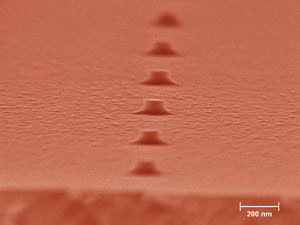
Using a combination of electron-beam lithography and wet etching,
they carve quantum dots from layers of semiconductor material. The result is a finely
aligned array of quantum dots set at a pitch of 500 nm to 5 µm. They have formed
quantum dots with diameters ranging from about 10 to 80 nm.

Using electron-beam lithography and wet etching
techniques, scientists at NIST carve quantum dots directly out of a semiconductor
substrate. Courtesy of Verun B. Verma, NIST.
Being able to change the size and pitch of these quantum dots
might be useful for displays because the emission wavelength produced by the particles
is tunable by size, Verma said. “With the etching technique, this can be done
in a deterministic way, with different regions of the same semiconductor chip producing
different colors of light.”
Currently, the NIST researchers are working with infrared outputs,
but Verma said that visible light might be possible.
Verma’s team reported its findings in the December 2010
issue of IEEE Journal of Quantum Electronics and in the Feb. 28, 2011, issue of
Optics Express.
Interview with Seth Coe-Sullivan, QD Vision Inc.
What are the latest advances in quantum dot displays?
I’d say that we’ve been pleasantly surprised at the
market’s reaction to quantum dot display demonstrators that we’ve made,
from handhelds to tablets to TVs which, if anything, has accelerated our anticipated
pace of product adoption. This is for quantum dots as down-converters in LED-based
LCD backlight units.
What are the short- and long-term goals for QD display technology
– in general and at QD Vision in particular?
We want to put QDs as down-converters into displays in 2012. The
quantum dot LED (QLED) electroluminescent displays will follow a couple of years
after that, and I think that having QDs in display applications already will be
a big credibility boost to the technology.
Are deposition techniques a hurdle, something to refine, or is
it “solved”?
I wouldn’t call it solved. We have been getting very nice
results with our patented contact printing method, and we believe this will scale
well to large areas. However, we have yet to demonstrate it at sizes truly relevant
for TV manufacturing, so that remains a milestone.
Is QD-as-LED the only path to success?
No, we believe that the QDs in lighting applications, and QDs
in display as applications, both in simple down-conversion mode, can be an independent
path to success for the company and the technology. QLED still has greater promise
for power efficiency and design freedom.
A couple of years ago, quantum dot-based displays were expected
to reach efficiency levels 10 times that of LCDs. Has that happened?
I’d say 10x LCD is still within reach. We’ve pushed
the efficiency of our devices up to the point that they are competitive with all
other light-emitting technologies, but we still feel that we can reach even higher
– for example, trying to reach that 10x milestone.
What stability or lifetime issues remain? Do you expect further
tweaking of core/shell materials?
Yes, further refinement of core/shell materials will continue
and is key to our progress in stability and lifetime. In down-conversion applications,
lifetime is already sufficient, even for solid-state lighting specifications, but
more improvement is necessary for QLED to be commercial.
What do you expect the market for quantum dot displays to be this
year and beyond?
This year it will be quite small, but I expect that, in 2012,
there will be multiple product launches, with explosive growth continuing in 2013.