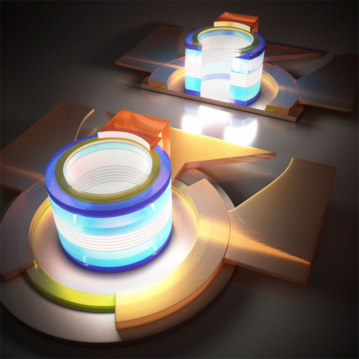
Record-small electrically pumped microlasers have been epitaxially grown on industry standard (001) silicon substrates. Continuous-wave lasing up to 100 degrees Celsius was demonstrated at 1.3 μm communication wavelength. Researchers achieved a submilliamp threshold of 0.6 milliampere for a microlaser with a radius of 5 μm. According to the team, these thresholds and footprints are orders of magnitude smaller than any previously reported lasers epitaxially grown on silicon (Si).

Schematic of the electrically pumped quantum dot micro-ring laser. Courtesy of Department of Electronic and Computer Engineering, HKUST.
Researchers grew a gallium arsenide (GaAs)-on-Si template using metal-organic chemical vapor deposition. V-grooves were defined on silicon substrates using patterned silicon dioxide (SiO2) as masks. An array of GaAs in-plane nanowires was grown inside silicon V-grooves by selective-area heteroepitaxy.
After the researchers removed the SiO2, further GaAs growth occurred. The GaAs nanowires were coalesced into a 1.5 μm thick continuous and smooth surface.
After metallization, the sidewall was passivated to further reduce surface recombination and diffusion. A SiO2 layer was sputtered to fully isolate the optical modes from the deposited metal pads. Contact probe pads were created for efficient current injection and spreading.
To measure the optical power, researchers collected radiation out-coupling from the micro-laser cavity through an integrating sphere at the side of the microlaser.
The research was performed by a team from the Hong Kong University of Science and Technology (HKUST) and the University of California, Santa Barbara. The team had previously collaborated on the development of CW, optically pumped microlasers operating at room temperature, epitaxially grown on Si with no germanium buffer layer or substrate miscut.
“Electrical injection of microlasers is a much more challenging and daunting task: first, electrode metallization is limited by the micro size cavity, which may increase the device resistance and thermal impedance; second, the whispering gallery mode (WGM) is sensitive to any process imperfection, which may increase the optical loss,” said researcher Yating Wan.

This advance underscores the continuous improvement and concurrent downsizing of transistors envisioned by Moore’s law, which predicted decades ago that the number of transistors in a dense integrated circuit would double approximately every two years, indefinitely.
“We demonstrated the smallest current injection QD lasers directly grown on industry-standard (001) silicon with low power consumption and high temperature stability,” said professor Kei May Lau. “The realization of high-performance micron-sized lasers directly grown on Si represents a major step toward utilization of direct III-V/Si epitaxy as an alternate option to wafer-bonding techniques as on-chip silicon light sources with dense integration and low power consumption.”
Future work will involve integration of in-plane coupling waveguides for efficient extraction and coupling of the lasing light. The team continues to work to make the overall performance of these micolasers comparable to or better than results achieved by bonding and to integrate these devices with high density in a compact, integrated optical communication system.
“As a promising integration platform, silicon photonics need on-chip laser sources that dramatically improve capability, while trimming size and power dissipation in a cost-effective way for volume manufacturability. The realization of high-performance micron-sized lasers directly grown on Si represents a major step toward utilization of direct III-V/Si epitaxy as an alternate option to wafer-bonding techniques,” said John Bowers, deputy chief executive officer of AIM Photonics.
The research was published in Optica, a publication of OSA, the Optical Society (doi: 10.1364/OPTICA.4.000940).