Focused ion beam electron microscopy is key for advanced nanotomography.
Dr. Edward L. Principe, Carl Zeiss SMT
The applications of focused ion beam-based nanotomography already are quite diverse and are expanding quickly. Materials science applications range from analysis of volumetric fractions of composition and porosity to crystallographic texture. Electronics industry applications include detailed failure analysis and three-dimensional visualization of complex nanoscale structures. Biomedicine and the life sciences are just beginning to tap into nanotomography via focused ion beam with special interest in ultrastructure within biological systems and in analysis of structures tagged with bioconjugated quantum dots.
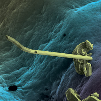
This microscopy image of a coated copper electrical connector shows a metal 'whisker,' which can grow up to a millimeter or more in length and has been known to cause electrical short failures in satellites.
The trend toward quantitative 3-D nanotomography is being advanced via a focused ion beam in conjunction with equipment to collect various analytical signals, such as electrons, x-rays, ions and photons. What traditionally was done in 2-D using a scanning electron microscope in the future will be accomplished with increasing frequency in 3-D through automated focused ion beam sectioning (Figure 1).
The rapidly maturing atom probe tomography method for materials characterization is another leading-edge quantitative nanotomographic technique. The focused ion beam platform facilitates automated sample preparation to provide significantly improved throughput in the same way focused ion beam has transformed transmission electron microscopy sample preparation.
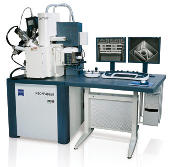
Figure 1. This instrument combines the functionality of a focused ion beam and a high-resolution scanning electron microscope. Ancillary components include a gas injection system to permit ion beam-assisted and electron beam-assisted chemical vapor deposition, x-ray detectors, micromanipulators, electrical test probes, advanced pattern generators, Fourier transform IR-Raman detectors and orientation imaging systems.
3-D volumetric characterization
The focused ion beam is a liquid metal ion gun (usually gallium ions) that uses an accelerated ion beam (1 to 30 kV, typically) focused via an electrostatic column. Scanning coils allow the ion beam to pattern or section virtually any material with nanoscale resolution. A focused ion beam may directly etch a pattern in a material with the ion beam, or it may perform patterned deposition of metals and oxides through ion beam-assisted chemical vapor deposition. The chemicals are delivered via a gas injection system built into the tool. This powerful platform continues to migrate at a rapid pace from its roots in the semiconductor industry into academic research and into diverse new industries in fields such as biology and the life sciences.
The ability to acquire, display and interrogate multidimensional volumetric data sets has been well established through various scientific disciplines. Common medical procedures such as computed tomography scans, MRIs and positron emission tomography scans have exposed the public to tomographic methods. A platform combining a focused ion beam and a scanning electron microscope can generate tomographic data, extending state-of-the-art imaging and analytical methods further into the third dimension.
The premise of the method involves sectioning the material using the focused ion beam in a sequential or continuous manner while acquiring various analytical signals to form an N-dimensional data set. Through standard reconstruction techniques, it is possible to assemble each “slice” of data into a 3-D volume. Depending upon the material and analytical signals collected, it is possible to achieve 5- to 20-nm resolution throughout the volume of a structure or device. The collected signals may be image data from secondary electrons, backscattered electrons, secondary ions, x-ray maps, backscatter diffraction patterns or Auger electrons, to name a few.
Focused ion beam-based nanotomography is more practical today because of advancement in the automation of the focused ion beam scanning electron microscope platform that has made the technique easier to use. Sectioning and signal collection can be entirely automated, allowing integration of multiple signals in a single experiment that can extend over several days. Postprocessing yields quantitative 3-D volumetric data, which is applied for visualization and for quantitative correlation between the structures, properties and performances of materials.
The advent of simultaneous imaging during the focused ion beam sectioning process with the CrossBeam platforms has made it practical to acquire several hundred continuous data frames in less than one hour in an automated way. This allows the capture of volumes of 500 μm or greater.
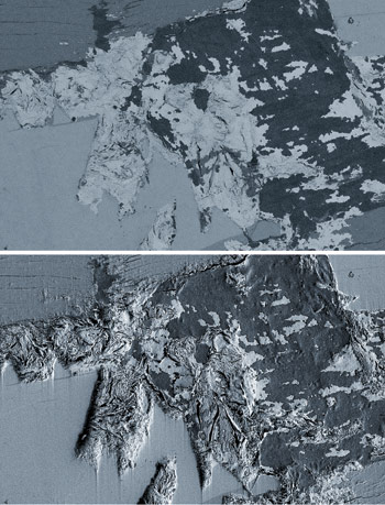
Figure 2. A comparison is shown of a low-voltage in-lens energy-selective backscatter image (top) and an Everhart-Thornley secondary electron image (bottom). Both images were collected simultaneously in a single scan from an uncoated geological material at 750 V. The backscatter image displays minimum topography and enhanced Z-contrast which, in many ways, is a perfect signal for electron nanotomography.
Low-voltage and energy-selective backscattered electron imaging is particularly beneficial for high-density nanotomography. Unlike traditional high-voltage backscatter imaging, low-voltage backscatter imaging uses on-axis in-lens detection principles to produce a viable high-resolution signal. The reason is that, at low voltage, the origination volume of the backscattered electrons is very similar to that of the emitted secondary electrons. Moreover, the on-axis energy-selective backscatter detector selectively images the high-angle low-loss backscattered electrons that experience single (or very few) scattering events. Hence, these backscatter electrons emit from close to the incident beam.
The systems require no detector insertion or alignment. The detector is always ready for use and can be used at a very short working distance. The energy-selective backscatter images (Figure 2) have a Z-contrast-weighted signal with minimum topographic (shadow) contrast, with minimum charging contrast and with minimum edge effect — the blooming sometimes seen in secondary images, which is caused by enhanced secondary production at edges.
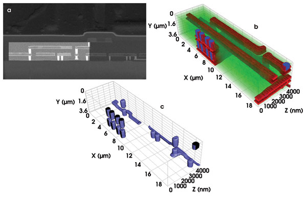
Figure 3. Focused ion beam 3-D nanotomography of a multilayer semiconductor device is shown using in-lens energy-selective backscatter detection. The backscatter image data stack was captured using a primary voltage of 0.8 kV. The energy-selective backscatter detector produces high-resolution Z-contrast, favorable for separating various materials in the 3-D reconstruction while suppressing voltage contrast and edge-enhanced contrast effects. (a) shows a single frame from the data set. (b) is a rendering of the entire volume where transparency has been applied to the interlayer dielectric (green) to highlight the metal interconnects (red) and the tungsten plugs (blue). In c, the isolated tungsten plugs are shown.
The low-voltage on-axis in-lens backscatter detection principle for focused ion beam-based nanotomography can be used on multilayer semiconductor devices such as the one in Figure 3. But the technique works equally well even for biological structures, whether critically point-dried or fixed and stained.
Advanced image processing, ranging from segmentation to feature counting and volumetric analysis also may be applied. Standard image processing in combination with specialized code has been applied to the 3-D volumetric analysis of fuel cells using focused ion beam nanotomography to quantify porosity, chemical composition and three-phase boundary lengths.
The future of focused ion beam-based nanotomography is predicted to grow in terms of complexity and in the range of applications. As any technology platform matures, the level of sophistication increases, but so, too, do the levels of automation and ease of use. The modern automobile is, perhaps, the quintessential example. Ultimately, the matured analytical platforms provide the required accessibility for more routine use. Focused ion beam-based nanotomography and its matured derivatives are expected to experience more routine use and to proliferate through-out various industries over the next several years.
Atom probe tomography is a rapidly maturing technology that also is enabled by focused ion beam preparation. The instrumentation is a combination of a field ion microscope and a time-of-flight mass spectrometer. In this technique, the position and identity of each extracted atom are mapped to the original volume of the sample, which consists of a sharp needle 100 to 150 nm in diameter. The method offers very high spatial resolution, but it is limited to within the predefined volume of the tip. Because the most versatile and dominant method for preparing atom probe tips uses a focused ion beam, atom probe tomography also can be considered a tomographic technique that is enabled by a focused ion beam.
Atom probe advantages
Although transmission electron tomography provides higher ultimate spatial resolution in terms of image data, atom probe tomography yields a nearly ultimate compositional spatial resolution. Both conductors and insulators may be analyzed with varying degrees of difficulty over volumes that can encompass an entire modern semiconductor device.
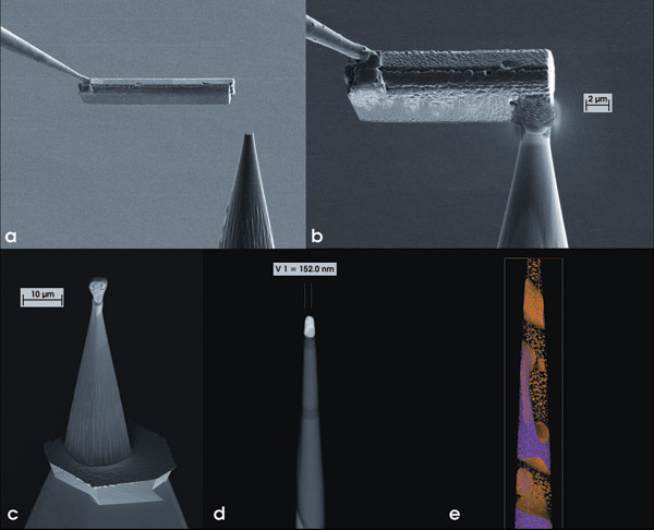
Figure 4. Parts a through d represent an abbreviated description of the focused ion beam preparation process for an atom probe sample using the Imago LEAP technique. The bright contrast region shown in panel d is actually a protective layer of platinum that previously was applied by ion beam-assisted chemical vapor deposition to protect the region of interest lying just beneath the platinum. Part e is representative data from the LEAP. For visual clarity, only a percentage of the total atoms detected is shown. The sample shows an isoconcentration line representing less than 90 percent iron toward the exterior and more than 90 percent on the interior. Part e is courtesy of Imago Scientific Instruments Corp.
For atom probe sample preparation, a basic method prescribed by Imago Scientific Instruments Corp. of Madison, Wis. — the manufacturer of the Local Electrode Atom Probe (LEAP) — can be used. The procedure is detailed, but the basics are discussed here. First, a wedge of material is cut from the sample and welded to an in situ micromanipulator via ion beam-assisted chemical vapor deposition. Typically, this section is on the order of 40 μm in length, and several identical specimens can be prepared from a strip of material. Once this section of material has been transferred via the micromanipulator to a microtip that is vertical, the sample attached to the manipulator approaches the tip from the left (Figure 4a). The distal end of the sample is then welded to the tip, again using ion beam-assisted metal chemical vapor deposition (Figure 4b).
The focused ion beam next is used to cut and separate the welded portion of the sample from the remaining portion of the strip still attached to the micromanipulator. A free-standing wedge of the sample material attached to the microtip results (Figure 4c). A series of focused ion beam milling operations forms the sample into a needlelike shape with a tailored shank angle and a diameter of 100 to150 nm (Figure 4d).
The final step involves low-voltage ion milling — usually at around 1 to 2 kV — to remove the protective platinum layer. The final steps are completed with the aid of live scanning electron microscope imaging during the milling process to carefully monitor the erosion of the platinum cap layer in real time. This imaging is critical for monitoring when just a minute amount of the protective cap layer is left. The low-voltage focused ion beam milling minimizes the amorphous damage produced by the ion bombardment and preserves the structure of the sample.
The prepared tip is aligned into the atom probe instrument for analysis. The tip is positioned close to an electrode, and a high electric field is maintained between the tip and the local electrode. An additional field that is approximately 10 percent above the nominal electrode field is pulsed at a high rate to extract atoms from the surface of the tip. With insulators or semiconductors the electric field pulse may be replaced by a laser pulse. The atoms are removed in a nearly sequential fashion with each energy pulse, and the position and identity of each detected atom are mapped throughout the volume with approximately 0.2-nm spatial resolution (Figure 4e).
The technique is intrinsically quantitative. One intriguing aspect of atom probe analysis is the variety of data mining that can be applied from a single data set. It is possible to construct virtual images similar to those produced by transmission electron microscopy along any plane as well as to construct quantitative profiles in any direction. The detection limits rival or exceed those realized with secondary ion mass spectroscopy, rendering atom probe analysis suitable for dopant profile characterization. The variety of heterogeneous compositions and materials systems that can be analyzed effectively by the method continues to increase, and in the future, much wider use of atom probe tomography is anticipated.
Acknowledgments
The author is grateful to Imago Scientific Instruments Corp. for permission to use the LEAP data shown and for helpful discussions.
Meet the author
Edward L. Principe is applications development manager in the North America Nano Technology Systems Div. at Carl Zeiss SMT in Melbourne, Fla.; e-mail: [email protected].