A near-IR imaging chip based on polycrystalline germanium on silicon opens new frontiers for integrated optoelectronics.
Lorenzo Colace, Gianlorenzo Masini, Valentino O. Cencelli,
Francesco de Notaristefaniand Gaetano Assanto, Nonlinear Optics and OptoElectronics Laboratory, Università Roma Tre
In the past two decades, SiGe has been the material of choice for the development of near-IR (0.7 to 2 µm) optoelectronic devices based on silicon, and several groups have developed high-performance near-IR photodetectors on Si substrates.1 Nevertheless, the gap between engineering a good device and achieving its monolithic integration with very large scale integrated electronics on Si was not overcome until recently.2
Following the pioneering work of R. People3 and T.P. Pearsall,4 SiGe (i.e., alloys, multilayers, superlattices, etc., that combine both of these group-IV semiconductors) has been an alternative to III-V compounds for the fabrication of near-IR optoelectronic devices monolithically integrated with silicon. Significant research efforts directed at Si-based sources, modulators and detectors, however, hit performance limitations both because of centrosymmetry and because of the indirect nature of band-to-band transitions in Ge. Moreover, silicon and germanium exhibit a lattice mismatch of approximately 4 percent.3
For a time, the primary motivation for the development of such near-IR detectors was fiber optic communications. More recently, the number of near-IR applications has increased dramatically, including new communications approaches, intrachip optical interconnects, spectroscopy and sensing in the presence of smoke or fog.5 These applications have established new requirements and have greatly reinforced the relevance of monolithic integration with silicon electronics.
To this extent, the advantage of Si-Ge compatibility can be best exploited in arrays of near-IR photodetectors, which rest on massive electronic circuitry for addressing, timing and processing. Because only silicon CMOS integrated circuits can meet the complex requirements of imaging devices, process compatibility is of paramount relevance.
Compatibility issues
Despite various demonstrations of Ge-based near-IR detectors on silicon,6-8 the combination of Ge epitaxy and device fabrication with silicon electronics is not an established technology. Technological compatibility is a rather involved issue: Many SiGe growth and processing techniques have been proposed, and very large scale integration is itself a complex, multistep and often proprietary process.
Although SiGe alloys with low Ge concentration are used in heterojunction bipolar transistors and the related technology is compatible with silicon CMOS devices, these materials are not suited for efficient near-IR detection because of the low absorption in that spectral range.9 A useful ground for discussion is the process flow of a consolidated CMOS technology, featuring a minimum feature size of 0.25 μm (Figure 1). The sequence and choice of materials and processing stem from a tight optimization, and a new step/material is a threat to the reliability of CMOS integrated circuits.
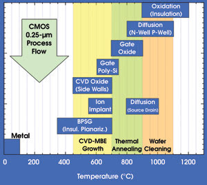
Figure 1. The silicon CMOS process flow includes typical temperature intervals (boxes) for the most relevant steps. Common temperatures for SiGe/Si heteroepitaxy are indicated by the color bands.
The figure points out a reduction in the allowed temperatures, based on a few critical effects: dopant diffusion above 700 °C, aluminum melting point at 660 °C, contact stability up to 500 °C and stability of planarizing materials up to 450 °C. Conversely, the growth of a Ge film with crystal quality suitable for near-IR photodetection implies a conspicuous thermal budget, the most critical steps being wafer cleaning (800 to 1000 °C), epitaxy (450 to 700 °C) and annealing (700 to 900 °C). To enlighten cross-incompatibilities, these ranges are indicated in the figure as vertical bands.
Merging standard very large scale integration and Ge/Si heteroepitaxy is difficult if we consider that Ge/Si suffers thermal stress related to an increased dislocation density and interdiffusion. In fact, neither strained nor relaxed heterostructures can tolerate the temperatures at which thermal oxidation and dopant diffusion are performed. Thus, monolithic integration must take place after the processes with highest thermal budgets (thermal oxidation and diffusion), assuming that further annealing is not required and that the cleaning of the silicon surface is carried out in earlier steps.
Polycrystalline germanium
The least invasive solution involves adding Ge layers as a back-end process, but this severely limits the maximum temperatures. A consolidated upper limit is about 450 °C; i.e., the maximum allowable for the chemical and physical stability of planarizing/insulating materials. In any case, without experimental data on chip robustness vs. temperature, a more conservative value is 350 °C.
An upper limit of 350 °C is a practical obstacle to most Ge/Si fabrication processes, the exception being the deposition of poly-Ge. Therefore, our group at Università Roma Tre in Rome has introduced the use of thermally evaporated Ge films that exhibit a polycrystalline morphology but the same optical absorption as single-crystal Ge when substrates are kept above 250 °C. This implies that a poly-Ge near-IR sensitive layer can be safely deposited onto Si electronics.10
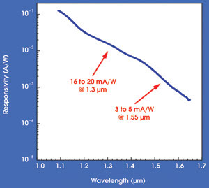
Figure 2. Spectral responsivity as measured in poly-Ge photodiodes on silicon extends up to 1.6 μm.
The electronic properties of poly-Ge on Si are affected by a large acceptorlike defect density (high P-type conductivity), which eliminates the need for doping but implies a short carrier lifetime. Nevertheless, the high near-IR absorption (about 104 cm–1 at 1.3 μm) makes this material promising for near-IR detectors. We have demonstrated heterojunction poly-Ge/Si photodiodes with a significant responsivity (16 mA/W at 1.3 μm), low dark current (1 to 3 mA/cm2) and high speed (>2.5 Gb/s).11 For a typical poly-Ge photodiode, spectral responsivity extends up to 1.6 μm (Figure 2), and rectifying response appears in its current-voltage characteristic (Figure 3).
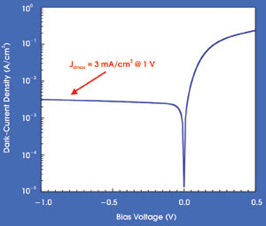
Figure 3. The current-voltage plot of a typical poly-Ge/Si photodiode shows a rectifying response. The arrow indicates the maximum dark-current density.
We are aiming at responsivities as high as 100 mA/W. But by adopting poly-Ge in place of crystal Ge, we do trade some near-IR sensitivity for integratability. The dark-current density and speed are more than adequate for most applications.
Near-IR integrated circuits
The poly-Ge near-IR integrated circuits offer some flexibility because of the low thermal budget. Moreover, experimental evidence suggests that temperatures above 600 °C do not appreciably affect the properties of poly-Ge. Nevertheless, to minimize the overall impact of a nonstandard process, we introduced the integration of poly-Ge on Si as the last fabrication step.
This near-IR integrated linear array of 64 pixels (Figure 4) was fabricated with standard silicon technology. The optoelectronic integrated circuit, equipped with analog-to-digital converters at each pixel, performs addressing and readout, yielding a real-time serial digital output.
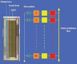
Figure 4. The integrated linear array of 64 pixels includes analog-to-digital converters at each pixel and circuits to perform addressing and readout.
The electronics specifically compensate for low detector sensitivity, using high-gain analog-to-digital conversion and a scheme to cancel dark currents. In the array, a poly-Ge diode is screened from light, and programmable digital-to-analog converters perform an accurate and individual calibration and real-time subtraction at each (illuminated) pixel to adjust dark current, thus enabling large amplifications.
The electronic front end of each detector contains an 8-bit double-ramp analog-to-digital converter, a 3-bit digital-to-analog converter and various current mirrors for dark-current cancellation. An externally selectable integration time between 1 μs and 50 ms enables circuit operation with photocurrents between 10 nA and 10 μA. For a responsivity of 10 mA/W, this corresponds to incident powers between 1 μW and 1 mW. The electronics can perform a complete cycle of integration, conversion and readout of the whole array in 64 μs, a standard interval in PAL television.
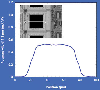
Figure 5. A single near-IR pixel (inset) exhibits its responsivity profile at 1.3 μm along the cross section (A to A).
To evaluate the impact of the nonstandard postprocessing, we tested the chip’s functionality (the response of the analog-to-digital converters to test currents) before and after Ge deposition. We found no changes after poly-Ge growth at 250 to 350 °C; i.e., the observed variations were always within the dispersion of the characteristics of unprocessed chips. The responsivity of individual integrated photodiodes was around 0.5 mA/W, with a photoresponse uniformity (within each pixel) of about ±2 percent and a better than 250 dB crosstalk between adjacent elements (Figure 5).
We are developing a two-dimensional array of 64 × 8 pixels with a similar architecture. Although pixel sensitivity can (and will) be improved, this near-IR imaging chip already opens new frontiers for integrated optoelectronics on silicon.
References
1. G. Masini et al (2001). Handbook of Thin Film Materials, Vol. 4. Hari Singh Nalwa, ed. Academic Press, p. 327.
2. G. Masini et al (May 6, 2002). Monolithic integration of near-infrared Ge photodetectors with Si complementary metal-oxide-semiconductor readout electronics. APPL. PHYS. LETT., pp. 3268-3270.
3. R. People (September 1986). Physics and applications of GexSi1-x/Si strained-layer heterostructures. IEEE J. Quantum Electron., pp. 1696-1710.
4. T.P. Pearsall (June 1989). Silicon-germanium alloys and heterostructures: optical and electronic properties. CRIT. REV. SOLID STATE MAT. SCI., pp. 551-599.
5. G. Masini et al (2004). Encyclopedia of Nanoscience and Nanotechnology, Vol. 3. Hari Singh Nalwa, ed.; Academic Press, pp. 829-842.
6. S.B. Samavedam et al (Oct. 12, 1998). High-quality germanium photodiodes integrated on silicon substrates using optimized relaxed graded buffers. APPL. PHYS. LETT., pp. 2125-2127.
7. L. Colace et al (March 6, 2000). Efficient high-speed near-infrared Ge photodetectors integrated on Si substrates. APPL. PHYS. LETT., pp. 1231-1233.
8. S. Famà et al (July 22, 2002). High performance germanium-on-silicon detectors for optical communications. APPL. PHYS. LETT., pp. 586-588.
9. Masini et al (2001).
10. Masini et al (May 2002).
11. G. Masini et al (April 14, 2003). 2.5 Gbit/s polycrystalline germanium-on-silicon photodetector operating from 1.3 to 1.55 µm. APPL. PHYS. LETT., pp. 2524-2526
Meet the authors
The authors are associated with the Nonlinear Optics and OptoElectronics Laboratory and INFN-Microelectronics Laboratory at Università Roma Tre in Rome; e-mail: [email protected].